Comprehensive guide to X-ray inspection systems in PCB manufacturing: How X-ray machines ensure quality, detect defects, and optimize electronics assembly
In the field of Electronics Manufacturing Services (EMS), the increasing complexity of Printed Circuit Boards (PCBs) has led to the demand for more advanced inspection technologies. Traditional inspection methods, such as manual visual inspection or even Automated Optical Inspection (AOI), often fall short when dealing with high-density interconnects, complex multi-layer boards, and components such as Ball Grid Arrays (BGAs). In these environments, X-ray inspection provides a non-destructive, high-resolution solution capable of detecting internal defects, misalignments, and voids that are otherwise invisible.
As EMS providers strive for the highest levels of quality assurance and compliance with industry standards, the use of X-ray becomes essential not only for detecting defects but also for supporting continuous quality control processes. X-ray-based techniques are uniquely suited for uncovering hidden solder joint failures, including insufficient solder, head-in-pillow defects, or bridging in BGAs and other bottom-terminated components. The integration of X-ray inspection systems into the production line enables comprehensive monitoring without disrupting throughput, thereby supporting both inline and offline inspection strategies.
The importance of X-ray inspection within EMS extends far beyond visual confirmation; it contributes directly to product reliability, minimizing the risk of latent failures and reducing post-manufacture service calls. As PCBs continue to evolve in complexity and density, the need for advanced systems like automated X-ray inspection grows proportionally, reinforcing their critical role in modern electronic production environments.
Conventional inspection methods, including AOI and functional testing, are often inadequate in detecting hidden defects that reside beneath opaque packages or inside multilayer PCB structures. As designs move toward tighter layouts and use of embedded components, relying solely on visual or electrical tests becomes increasingly insufficient. AOI may detect surface-level anomalies but cannot penetrate solder joints or inspect the internal layers of the printed circuit board.
X-ray inspection fills this critical gap by enabling the visualization of inner structures through radiography, without damaging the component or PCB itself. By utilizing controlled radiation dose and sensitive detectors, X-ray devices can reveal misaligned connections, solder voids, and open circuits that would otherwise pass undetected. The ability to detect and quantify these defects is particularly crucial in industries where failure is not an option, such as aerospace and medical electronics.
Additionally, certain testing technologies, like boundary scan test, are limited in scope and cannot assess physical assembly issues, such as insufficient solder or contamination. Even functional test setups may fail to isolate intermittent or mechanical failures. In contrast, X-ray and CT systems provide a detailed 2D or 3D inspection view, depending on the system configuration, offering engineers an unparalleled tool for in-depth analysis.
As a result, X-ray inspection is now considered an industry standard in PCB manufacturing, particularly for inspecting assemblies with BGAs, connectors, and other components where optical access is limited. The increasing reliance on inspection capabilities that include non-destructive testing (NDT) highlights the irreplaceable role of X-ray inspection equipment in ensuring quality X-ray validation and meeting the demands of high-reliability production.
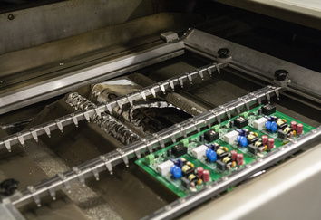
An X-ray inspection system used in PCB manufacturing consists of several critical components that work together to enable accurate and non-destructive evaluation of soldered connections and internal board structures. At the core is the X-ray source, which generates a tightly focused beam of radiation directed at the object under inspection. The beam penetrates the PCB and its components, and the varying absorption rates of different materials allow for contrast in the resulting radiographic image.
Opposite the source is the detector, which captures the X-ray image. The quality of the image is dependent on the resolution of the detector, the energy of the X-ray beam, and the geometrical configuration of the system. Flat-panel detectors are commonly used due to their sensitivity and ability to operate at high frame rates, which supports real-time analysis. These detectors convert X-rays into digital signals, making it possible to visualize fine structures such as internal solder fillets, voids, and incomplete joints.
Modern systems also integrate precise mechanical stages that allow for dynamic positioning of the board and rotation of the sample, especially in advanced 2D and 3D applications. Software is another vital component, providing not only image reconstruction but also tools for defect detection, statistical analysis, and pass/fail classification. High-end systems may incorporate artificial intelligence to improve detection accuracy and reduce operator variability.
Together, these components form a robust inspection system capable of revealing hidden defects in high-density PCBs. Such systems are indispensable for identifying structural issues that cannot be observed through surface inspection techniques.
There are various types of X-ray systems employed in the inspection of PCBs, each designed to meet specific requirements in terms of resolution, inspection depth, and automation. The most common categories are 2D X-ray and 3D computed tomography systems.
A 2D X-ray system captures a flat image of the object, providing a quick and effective way to inspect large volumes of PCBs for standard assembly defects. These systems are often used for inline inspection and support high throughput applications. They are capable of detecting solder volume variations, bridging, insufficient wetting, and misaligned components. Despite their simplicity, 2D systems remain highly effective in many production scenarios and are often used in combination with automated optical inspection to cover both internal and external defect types.
For more complex boards, particularly those with stacked components or embedded structures, 3D systems based on X-ray CT are employed. These systems generate a volumetric reconstruction of the object by taking multiple radiographic images at various angles and reconstructing a 3D model. The added depth information allows for inspection of specific layers of the PCB, making it possible to detect voids, delamination, or cracks in solder joints that are completely obscured in a 2D image.
Some inspection systems are hybrid in nature, combining 2D and 3D capabilities. These are particularly useful in EMS environments where multiple product types are produced, requiring flexibility in inspection depth and accuracy. Advanced X-ray inspection solutions of this kind represent the current frontier of nondestructive testing in the electronics industry.
The choice between X-ray machines and optical inspection depends largely on the nature of the defects being targeted and the accessibility of the features on the board. Optical inspection methods, including automated optical inspection, are well-suited for identifying surface-level defects such as incorrect component placement, polarity issues, and missing parts. These methods rely on visible light and high-resolution cameras, making them fast and non-invasive, but they are fundamentally limited to what can be seen from the outside.
In contrast, X-ray machines excel at revealing internal structures, making them indispensable for evaluating solder joints under BGAs and other hidden interconnects. These machines can inspect multi-layer PCBs and detect problems such as voids, insufficient solder, and internal bridging. Optical systems may flag anomalies in shape or alignment, but they cannot assess internal connection quality, which often leads to latent reliability issues if left unchecked.
While both inspection technologies serve valuable roles in EMS operations, X-ray inspection systems are required wherever hidden or internal features are critical to product integrity. In many cases, they are used alongside optical systems to create a comprehensive inspection process that covers all failure modes, both visible and concealed. The integration of both approaches improves overall inspection coverage and contributes to more effective quality control across the manufacturing line.
The evolution of X-ray technology in electronics manufacturing has introduced increasingly sophisticated techniques for examining complex assemblies. The two primary modalities—2D X-ray and 3D computed tomography—each offer unique capabilities for defect analysis and structural evaluation.
2D X-ray inspection remains the most commonly deployed technique in high-volume environments due to its speed, simplicity, and effectiveness. By generating a single planar radiographic image, this method allows inspectors to detect a wide range of anomalies including solder voids, insufficient fill, bridging, and misalignment. Its speed and relatively low cost make it ideal for in-line inspection in SMT production, where high throughput and real-time process feedback are essential.
However, 2D images present a superimposed view of all layers, which can obscure certain critical features in dense assemblies. This limitation is addressed by 3D X-ray CT systems, which produce volumetric data through the acquisition of multiple projection images taken at different angles. These are then computationally reconstructed to form a three-dimensional model of the assembly. The result is a clear view into specific layers and individual solder joints, making it possible to identify internal defects such as head-in-pillow conditions or delamination that are difficult or impossible to isolate using 2D techniques alone.
While 3D X-ray CT offers superior visualization and inspection depth, it requires longer acquisition and processing times. As such, it is more commonly applied in failure analysis, prototype verification, and low-volume, high-complexity production runs. In many EMS environments, both 2D and 3D methods are used strategically depending on product type, defect risk, and inspection objectives.
CT-based inspection solutions have become an essential tool for analyzing the internal structure of PCBs and detecting defects that are not accessible through surface analysis. These systems utilize X-ray CT to generate highly detailed cross-sectional images and three-dimensional reconstructions of electronic assemblies. This capability is particularly important in the inspection of advanced components such as BGAs, chip-on-board structures, and embedded passives, where failure modes often originate beneath the surface.
The precision offered by CT systems enables accurate measurement of solder joint volume, detection of internal voids, and analysis of structural integrity in multilayer assemblies. Unlike traditional 2D methods, CT allows for the separation of overlapping features, which is crucial when inspecting densely packed PCBs or when verifying the assembly of stacked components. This separation is achieved by reconstructing multiple slices through the Z-axis, enabling precise identification of individual defects within the complex internal geometry of the board.
In addition to identifying production-related faults, CT-based inspection is often employed during root cause analysis and process optimization. It supports advanced inspection capabilities such as quantitative porosity analysis, measurement of bond line thickness, and verification of critical mechanical interfaces. These inspection solutions play a key role in industries where reliability is paramount and defects must be characterized with microscopic accuracy.
The implementation of X-ray CT systems is supported by continual improvements in detector resolution, faster image reconstruction algorithms, and greater automation. As these technologies evolve, CT-based systems are becoming more accessible to EMS providers seeking to enhance quality assurance and gain deeper insight into complex board structures.
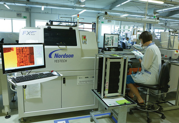
In the context of high-volume PCB manufacturing, automated X-ray inspection systems provide a scalable and reliable method for ensuring consistent assembly quality. These systems are designed for full integration into SMT production lines, enabling continuous inspection of each board without slowing down throughput. Automation eliminates operator subjectivity and reduces inspection time, which is critical in environments driven by cost-efficiency and fast cycle times.
Automated X-ray inspection systems can be configured to detect a broad range of defect types, including voids, insufficient solder, bridging, tombstoning, and misaligned components. With programmable inspection criteria and advanced image processing algorithms, they are capable of classifying defects in real-time and triggering corrective actions within the line. This capability allows manufacturers to maintain strict process control and prevent the accumulation of latent defects in downstream operations.
These systems often utilize high-speed 2D imaging in conjunction with limited-angle 3D views for targeted analysis. In some cases, adaptive inspection strategies are applied, where only specific regions of interest are inspected with greater resolution based on risk analysis or historical defect patterns. This hybrid approach ensures that inspection resources are applied efficiently without compromising accuracy.
The adoption of automated X-ray inspection also supports traceability, as each inspected board is logged with its corresponding image data and inspection results. This data can be analyzed to identify trends, optimize soldering parameters, and enhance predictive maintenance strategies. Over time, this leads to improved yield, reduced scrap rates, and better control over the entire manufacturing process.
As the complexity of PCBs increases, the value of automated systems lies not only in their ability to inspect but also in their integration with broader factory systems. The synergy between inspection and testing, real-time analytics, and intelligent feedback loops defines the modern standard for quality management in high-volume EMS production.
One of the primary benefits of X-ray inspection in PCB assembly is its ability to detect internal defects that are inaccessible through external inspection methods. These defects often originate in solder joints or multilayer interconnects and can compromise the electrical integrity or mechanical reliability of the assembly. Common issues include voids within solder joints, which can result in thermal or mechanical failure, as well as insufficient solder volumes, which may lead to intermittent connections or open circuits.
Bridging defects, where solder unintentionally connects two adjacent pads or leads, are also frequently observed through X-ray. These defects may be entirely hidden under packages like BGAs or QFNs, where no optical method can provide reliable verification. Head-in-pillow defects, a result of poor wetting between the solder ball and paste, are another critical issue detectable through radiographic analysis. These defects may pass initial functional tests but lead to early failure in the field.
In the highly dynamic environment of Electronics Manufacturing Services, the decision to implement inspection processes internally or rely on third-party inspection services depends on multiple operational and technical factors. In-house inspection systems offer immediate access to quality data, improved process integration, and rapid response to anomalies. These benefits make internal solutions attractive for manufacturers seeking real-time defect identification and closed-loop process control.
However, establishing and maintaining internal inspection capabilities can be capital-intensive. High-end X-ray systems require skilled operators, regular calibration, and dedicated space, particularly when advanced equipment such as X-ray and CT systems are involved. Outsourced inspection services provide an alternative path, particularly for low-to-medium volume runs, prototype builds, or manufacturers without sufficient technical infrastructure. These service providers often possess a wider range of inspection devices, including non-destructive testing technologies that may not be cost-effective for individual facilities to acquire.
The choice ultimately depends on product complexity, regulatory compliance requirements, and the need for traceable inspection data. For highly regulated industries such as aerospace or medical electronics, outsourcing to labs with certified quality systems may provide both technical depth and compliance assurance. Conversely, high-volume EMS providers may find greater value in integrating advanced inspection systems directly into their lines, especially where product inspection solutions must be tightly coupled with production throughput and cost efficiency.
Regardless of the approach, the goal remains the same: to ensure reliable detection of manufacturing defects, to validate process stability, and to support long-term product quality through rigorous inspection and testing practices.
Professional product inspection solutions extend far beyond basic defect detection. These systems provide detailed insights into the physical and structural quality of electronic assemblies, supporting process optimization and long-term reliability. Among the key advantages is the ability to apply non-destructive methods, such as radiography and X-ray CT, across different stages of the manufacturing process, from early prototyping through to final product verification.
Advanced inspection solutions incorporate high-resolution detectors and intelligent software that enable automated analysis of critical features. They support classification of defect types, quantification of solder volumes, and evaluation of connector integrity. In particular, the integration of software-assisted pattern recognition and AI algorithms allows for consistent application of acceptance criteria, reducing human error and increasing inspection repeatability.
One of the most valuable aspects of modern product inspection solutions is their role in predictive quality management. By aggregating inspection data over time, manufacturers can identify trends, track performance of specific soldering processes, and implement proactive adjustments to prevent defects before they occur. This ability is fundamental to achieving high yield rates and complying with quality assurance systems required in global supply chains.
Product inspection solutions also facilitate documentation and traceability, which are critical in sectors where auditability and regulatory compliance are essential. By archiving detailed inspection records, EMS providers can support warranty processes, demonstrate compliance with customer requirements, and improve their responsiveness to service calls related to field failures.
The use of X-ray in these systems enables imaging of inner structures that would otherwise remain inaccessible, allowing for the detection of hidden defects such as micro-cracks, delamination, and incomplete soldering. This level of diagnostic power supports both production quality and long-term reliability of electronic products, especially in demanding environments.
When selecting an external provider of inspection services, EMS companies must evaluate several critical factors to ensure the provider’s capabilities align with their product complexity and quality objectives. A fundamental requirement is access to state-of-the-art inspection equipment, including industrial X-ray inspection systems that can detect fine structural anomalies without damaging the board.
In addition to equipment, the expertise of the inspection team plays a decisive role. Skilled inspectors who understand the intricacies of SMT and THT processes can identify subtle variations that generic analysis might overlook. Certifications, adherence to international inspection standards, and documented quality control procedures are also indicators of a provider’s reliability and professionalism.
Another important aspect is the range of services offered. Providers that offer both 2D and 3D imaging, as well as nondestructive testing using radiography, can accommodate a wider range of board types and defect profiles. Furthermore, the ability to generate comprehensive inspection reports, complete with annotated X-ray images and root cause assessments, adds value to the inspection process and supports continuous improvement initiatives.
The most effective inspection partners act not only as evaluators but also as contributors to quality strategy. Their input can help identify upstream process flaws, recommend corrective actions, and provide insights into design-for-inspection practices. In this sense, inspection services are not simply a compliance function but an integrated element of the broader quality ecosystem in electronics manufacturing.
X-ray inspection also allows engineers to detect component misalignments, solder displacement, and deformation, all of which may result from process instabilities. The clarity and precision of X-ray images make it possible not only to detect the presence of such anomalies but also to evaluate their severity and potential impact on product performance. As a non-destructive method, X-ray can be applied during any phase of production without damaging the board, enabling real-time corrective actions and continuous improvement of manufacturing processes.
In modern PCB manufacturing, X-ray detection has become integral to maintaining stringent quality control standards. Traditional methods of verification, while still valuable, often lack the resolution or internal visibility required to confirm solder joint integrity, especially in high-density or double-sided assemblies. With X-ray systems, manufacturers gain the ability to detect and classify a wide variety of internal defects with minimal operator influence, thereby enhancing consistency and repeatability.
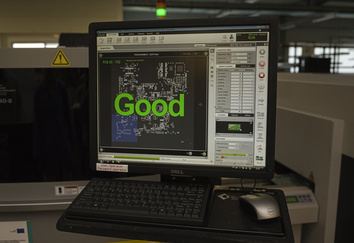
The inspection process typically involves capturing a series of X-ray images from different regions of the board, which are then analyzed either manually by an inspector or automatically through advanced software. These systems can detect fine variations in solder geometry, identify missing or misplaced components, and flag critical anomalies for further review. For example, by examining the sides of the PCB during inspection, engineers can observe joint profiles, layer structures, and the presence of embedded elements that would otherwise go unnoticed.
Through continuous monitoring enabled by X-ray inspection systems, manufacturers can establish traceable data for each PCB produced, allowing for thorough documentation and long-term analysis. This level of control contributes to both short-term defect reduction and long-term process stability. Over time, the adoption of high-resolution X-ray imaging has proven to be a valuable investment in improving yield, minimizing rework, and strengthening customer confidence.
In sectors such as aerospace, where quality control is paramount, the role of X-ray inspection becomes even more critical. The ability to confirm the structural integrity of every solder joint ensures that assemblies meet both internal quality standards and regulatory requirements. By integrating X-ray technology into the broader ecosystem of product inspection solutions, manufacturers can align with best practices for quality assurance and maintain competitive advantage in precision-driven industries.
While specific organizational examples are beyond the scope of this discussion, industry-wide research has consistently shown that implementing comprehensive X-ray inspection processes leads to measurable reductions in defect rates. Facilities that rely on visual and optical inspection alone often report a higher incidence of latent failures, particularly in products with complex or densely populated layouts.
By contrast, manufacturers that integrate advanced X-ray inspection equipment report improved detection of critical defects, such as incomplete solder joints and hidden shorts, early in the production cycle. This early detection not only prevents defective boards from reaching customers but also provides real-time feedback to process engineers, enabling immediate adjustments to reflow profiles, solder paste deposition, or component placement parameters.
The transition from traditional inspection devices to high-resolution X-ray inspection systems can reveal patterns in defect formation that were previously undetectable. For instance, voids caused by process variations may be systematically identified and traced back to material inconsistencies or equipment misalignment. This diagnostic capability strengthens root cause analysis and supports data-driven decision-making across the manufacturing line.
Ultimately, the implementation of PCB X-ray inspection contributes to higher first-pass yields, reduced reliance on post-production testing, and more efficient resolution of quality concerns. As inspection capabilities continue to evolve, X-ray remains one of the most effective tools for detecting defects and enforcing quality standards in the electronics manufacturing industry.
The aerospace industry imposes some of the most stringent quality requirements in electronics manufacturing, driven by the need for long-term reliability, high performance under extreme conditions, and full traceability. In this context, X-ray inspection technology plays a central role in validating the structural integrity of PCBs and identifying even the smallest anomalies that could compromise functionality in mission-critical environments.
Using an X-ray system allows engineers to inspect internal solder joints, assess the geometry and consistency of connections, and reveal hidden defects that could lead to latent failures during flight or under thermal and mechanical stress. The detection of defects in aerospace electronics is not merely a quality control task—it is a safety imperative. Because components are often densely packed and utilize advanced interconnection technologies, only high-resolution X-ray inspection systems can detect the full spectrum of fault conditions without damaging the assembly.
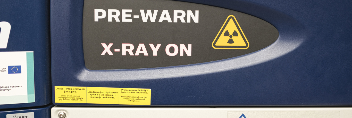
Aerospace manufacturers also require full radiation control within the inspection environment to protect both personnel and sensitive devices. As part of compliance with industry standards, X-ray equipment used in these sectors must be precisely calibrated, shielded, and validated for repeatable performance. These practices ensure that every layer and solder joint within a complex PCB can be evaluated without compromise. The integration of automated scanners and image recognition software further enhances consistency across large batch evaluations, enabling detailed reporting and process documentation.
In this sector, the contribution of leading X-ray solutions extends beyond inspection. These technologies support diagnostic workflows, facilitate failure analysis, and serve as verification tools during environmental and life-cycle testing. Ultimately, the role of X-ray in aerospace is embedded in a broader framework of design validation, process control, and long-term operational reliability.
Beyond aerospace, X-ray inspection systems are widely used in other safety-critical industries, such as medical devices and automotive electronics. In medical electronics, patient safety and regulatory compliance demand extremely low defect rates and rigorous testing protocols. X-ray equipment is applied to inspect solder joints beneath BGAs, verify the position and integrity of microelectronic components, and detect voids that could compromise signal integrity or thermal transfer.
Automotive electronics, especially in applications related to autonomous driving and powertrain management, are increasingly reliant on dense packaging and advanced interconnection methods. These assemblies are subject to vibration, thermal cycling, and mechanical loads, making the detection of structural imperfections a fundamental requirement. In both sectors, X-ray inspection systems can detect hidden discontinuities, insufficient solder, internal bridging, and micro-fractures that may not be visible through optical means or standard functional testing.
Detection systems in these applications are often integrated with automated handling and image processing tools to support high-volume, consistent inspections. Furthermore, service X-ray processes may be employed in maintenance and diagnostic contexts to examine returned or failed units without disassembly. This non-destructive approach enables root cause analysis and supports decisions regarding product repair or replacement, helping to reduce warranty costs and enhance overall reliability.
In addition, metal detector technology is occasionally combined with X-ray imaging to validate component presence and foreign material contamination, particularly in hybrid manufacturing environments. The use of such hybrid approaches reflects a growing emphasis on multilayer detection strategies across a wide range of industries.
In industrial and consumer electronics, the inspection requirements can vary significantly based on product complexity, expected life span, and functional safety requirements. However, as integration density increases and margins for error shrink, more manufacturers are turning to advanced X-ray inspection systems to ensure consistent production outcomes.
These systems provide critical visibility into solder integrity, component alignment, and internal mechanical structures. Especially in high-density applications involving integrated circuits (ICs), the ability to capture X-ray images of internal interconnects without interfering with the assembly is essential. In many cases, X-ray inspection technology is the only viable method to identify solder-related anomalies, such as delamination, voids, or bridging beneath component packages.
One of the key advantages of these inspection systems is their versatility. A modern X-ray system can be configured to inspect a broad array of product types, including rigid, flexible, and hybrid PCBs. In some environments, dedicated inspection cells are equipped with programmable scanners, capable of inspecting multiple board sizes and configurations without extensive manual setup. These features support agile production strategies and high throughput requirements.
The ability to apply nondestructive testing across product lines also aids in predictive maintenance and quality monitoring. Detection of defects at early stages prevents downstream issues, minimizes rework, and supports higher first-pass yields. In environments where fast turnaround is essential, automated inspection systems enable rapid evaluation without sacrificing accuracy.
Whether deployed in industrial automation controls, personal electronics, or smart devices, inspection systems serve as a foundational layer of quality infrastructure. The flexibility, resolution, and depth offered by advanced X-ray equipment make it an essential part of quality assurance and risk mitigation strategies in today’s interconnected production ecosystems.
In modern surface-mount technology, components such as Ball Grid Arrays and Quad Flat No-lead packages have become standard due to their compact size and high pin density. However, their design presents a significant challenge for quality inspection, as the solder joints are located underneath the package, rendering them invisible to conventional optical methods. In these cases, using an X-ray is not only beneficial but necessary for inspecting the quality of hidden connections.
X-ray inspection systems can detect a variety of solder-related anomalies, including voids, bridging, insufficient wetting, and misalignment of pads and balls. These systems allow for detailed analysis of solder volume distribution and enable engineers to verify the presence of all connections beneath the component without disassembly. The visualization of BGAs through X-ray imaging provides critical insight into the mechanical integrity of each solder joint, making it possible to detect subtle defects that may otherwise go unnoticed until functional failure occurs.
Beyond BGA inspection, X-ray imaging is also used to validate solder joints on components mounted on the bottom side of the PCB or in densely populated areas where traditional probes cannot reach. This non-destructive testing method ensures that internal features are examined thoroughly and efficiently, without compromising the board's integrity.
Although not as common in standard PCB assembly, certain specialized boards include welded elements or interconnects, particularly in high-power or mechanically reinforced applications. In these cases, weld quality directly influences product reliability, especially in environments subject to vibration, temperature variation, or mechanical stress.
X-ray inspection technology provides a reliable solution for assessing welds within electronic assemblies. By generating detailed radiographic images of the joint, it becomes possible to identify porosity, incomplete fusion, internal cracks, and other discontinuities that could affect the mechanical or electrical performance of the weld. These inspections are often performed as part of advanced quality assurance procedures in critical applications such as aerospace systems, industrial power control units, or defense electronics.
The detection of such structural anomalies through X-ray imaging supports long-term product durability and helps meet industry requirements for safety and certification. In certain cases, CT imaging may be used to enhance the accuracy of weld analysis, especially when joints are multi-layered or difficult to access. X-ray-based inspection of welds exemplifies how non-destructive methods contribute to comprehensive quality control strategies in specialized electronics manufacturing.
In high-reliability applications, the ability to conduct non-invasive reliability testing is essential for validating the performance of solder joints and interconnects over time. X-ray and CT systems are frequently used to assess assemblies before and after environmental stress testing, such as thermal cycling, mechanical shock, or humidity exposure.
These systems provide high-resolution images of the solder joint structure, enabling the detection of micro-cracks, delamination, and solder fatigue that may develop during testing. By comparing X-ray images captured before and after stress exposure, engineers can quantify structural changes and better understand failure mechanisms that are not apparent through electrical testing alone.
In addition, X-ray imaging supports the inspection of conformal coating integrity, void migration, and internal corrosion in long-life products. This level of insight plays a key role in product qualification, especially in industries where failure could result in system downtime, injury, or mission loss.
CT-based systems further enhance reliability assessments by providing volumetric data that can be analyzed over time. They allow for layer-by-layer inspection of the PCB and its components, offering a deeper understanding of structural changes at the micro level. As part of a holistic inspection process, these tools are invaluable in supporting robust design validation and ensuring long-term performance of electronic assemblies.
As electronics manufacturing continues to evolve, one of the most significant advancements in X-ray inspection systems lies in the integration of artificial intelligence and machine learning algorithms. These technologies are being used to enhance detection precision, reduce false calls, and support real-time decision-making within inspection workflows. By training models on vast libraries of defect images, AI-powered systems are able to recognize complex fault patterns, learn from historical process data, and improve the consistency of classification across different product types.
AI is particularly effective in analyzing subtle variations in solder profiles, detecting emerging trends in defect occurrence, and highlighting regions of interest that may require closer scrutiny. As a result, inspection capabilities are no longer limited to defect detection alone, but extend into predictive quality control, process optimization, and intelligent resource allocation. These advancements also enable adaptive inspection strategies, where the system modifies its scanning behavior based on board complexity, prior defect history, or specific high-risk components.
The application of AI in X-ray systems represents a major shift in how quality assurance is performed, particularly in high-volume EMS environments where data-driven decision-making is critical for yield improvement and cost control.
The growing use of connected inspection platforms has led to the development of cloud-based data analytics systems, which allow manufacturers to centralize, compare, and analyze inspection results across multiple production sites. These systems collect data from X-ray inspection equipment in real time and store it in secure databases for ongoing analysis. By leveraging large datasets, engineers can monitor defect trends, compare machine performance, and implement best practices across the organization.
One key advantage of this approach is enhanced traceability. With centralized storage, each board's inspection history including captured X-ray images, defect annotations, and operator decisions—can be reviewed, audited, and analyzed at any time. This capability is especially valuable in industries that require rigorous documentation, such as aerospace or medical electronics, and supports root cause analysis in the event of product returns or field failures.
These analytics platforms also integrate with enterprise systems such as Manufacturing Execution Systems (MES) and Product Lifecycle Management (PLM) tools. This integration provides a holistic view of the inspection process, bridging the gap between design, manufacturing, and field performance. As a result, manufacturers can identify systemic issues faster and implement more effective corrective actions.
The shift toward cloud-based analytics also supports continuous improvement by identifying patterns in defect types, correlating defects with specific processes or materials, and providing data to guide design-for-manufacturing decisions. In this context, inspection becomes not just a checkpoint, but a continuous feedback mechanism for operational excellence.
Looking ahead, the future of X-ray inspection is closely tied to automation, scalability, and intelligent control. Next-generation X-ray systems are expected to offer even faster scanning speeds, higher resolution imaging, and deeper integration with smart manufacturing systems. These developments aim to reduce inspection time without sacrificing accuracy, making it feasible to inspect every PCB in high-throughput production lines.
Future systems will rely increasingly on automated detection algorithms that are self-optimizing and capable of learning in real time. These algorithms will not only detect defects, but also suggest corrective actions, prioritize urgent issues, and optimize line performance based on inspection outcomes. This level of automation is crucial for supporting the production of complex assemblies involving a wide variety of component packages, such as BGAs, ICs, and connectors.
In addition to speed and accuracy, upcoming systems will place greater emphasis on radiation control and safety. As X-ray usage increases across a wide range of industries, maintaining strict radiation dose limits while improving image quality will be an ongoing challenge. Innovations in source technology, shielding, and sensor materials are expected to address these concerns, making high-resolution imaging safer and more efficient.
Another anticipated trend is the convergence of multiple inspection technologies into unified platforms. Future product inspection solutions may combine optical, X-ray, and functional testing in a single inspection station, reducing equipment footprint and increasing process flexibility. The coordination of these technologies will allow manufacturers to inspect all relevant aspects of a PCB from surface conditions to internal structures and electrical behavior within one continuous process.
These integrated systems will act as intelligent detection hubs, using advanced software to correlate data from various inspection devices. By cross-referencing multiple inspection outputs, they will deliver deeper insight into process variability, enhance detection of subtle structural changes, and strengthen overall quality assurance.
Ultimately, the future of X-ray inspection in EMS is defined by the pursuit of accuracy, speed, and connectivity. With advances in X-ray source design, smarter detection systems, and seamless data integration, X-ray inspection will remain a central pillar of quality infrastructure in electronics manufacturing.
In the landscape of modern electronics manufacturing, X-ray inspection has become indispensable for ensuring product reliability, verifying structural integrity, and maintaining consistent quality in high-density, multilayer PCB assemblies. As the complexity of surface-mount and through-hole components increases, and as the miniaturization of designs becomes more pronounced, traditional inspection methods alone are no longer sufficient to guarantee defect-free assemblies.
X-ray machines, both 2D and 3D, have proven to be powerful tools for visualizing hidden solder joints, internal layers, and microscopic defects that may not affect immediate functionality but pose a significant risk to long-term reliability. The ability of X-ray inspection systems to detect issues such as solder voids, bridging, head-in-pillow defects, and delamination underscores their central role in a comprehensive quality assurance strategy. When combined with automated optical inspection and functional test methods, these systems form a robust inspection and testing ecosystem capable of identifying both visible and concealed faults across the production process.
One of the most significant contributions of X-ray technology is its adaptability. Whether deployed in prototype validation, process monitoring, or final quality verification, X-ray systems enhance diagnostic precision and support faster feedback loops between inspection and process control. The integration of X-ray source advancements and intelligent detection systems continues to improve resolution, reduce cycle times, and enhance the detection of subtle anomalies. These developments have given rise to a new generation of advanced systems that are both more efficient and more aligned with the principles of smart manufacturing.
Quality assurance in electronics is no longer a static checkpoint but a dynamic, data-driven process that relies heavily on real-time imaging and analysis. The evolution of X-ray inspection technology, especially in the form of AI-assisted detection and cloud-based analytics, is transforming how manufacturers monitor and respond to process variation. These tools not only improve throughput but also reduce false positives, streamline corrective actions, and enable traceable decision-making—all essential for sustaining competitive advantage in global markets.
The versatility of X-ray inspection is further evident in its adoption across a wide range of industries, including aerospace, medical, automotive, industrial automation, and consumer electronics. Whether inspecting the fine interconnects of ICs, validating the structural integrity of connectors, or analyzing solder joint reliability under mechanical stress, X-ray imaging supports a high level of diagnostic confidence that few other inspection methods can match.
Looking forward, the synergy between X-ray devices, automated systems, and intelligent software will define the next generation of product inspection solutions. The continued integration of nondestructive testing methodologies, enhanced scanner functionality, and greater inspection capabilities will allow manufacturers to address hidden defects early, improve first-pass yield, and reduce the need for costly rework or field service X-ray diagnostics.
To remain aligned with industry standards and customer expectations, manufacturers must embrace inspection systems not as isolated tools, but as core components of their process infrastructure. X-ray inspection, with its unmatched ability to visualize the unseen, will remain a leading X-ray methodology for ensuring structural integrity, product safety, and long-term field performance. In the era of high-mix, high-speed electronics production, optimizing inspection with X-ray technology is not just an advantage it is a necessity.