Mastering THT Wave Soldering: Design, Process, and Selective Wave Soldering Best Practices for PCB Assembly
As the electronics industry continues to evolve toward higher performance, miniaturization, and increased functional complexity, manufacturing methods must adapt to meet both technical and economic demands. While Surface Mount Technology (SMT) dominates much of modern assembly, Through-Hole Technology (THT) and its related soldering processes, particularly wave soldering and selective wave soldering, remain essential in critical applications requiring durability, high current capacity, and thermal stability.
This article provides a comprehensive and technical exploration of THT soldering, the mechanics of wave soldering systems, and the innovations driving selective wave soldering. It covers design rules, process optimization, quality assurance techniques, and emerging trends that will define the future of PCB assembly in high-reliability environments. Aimed at engineers, designers, and manufacturing professionals, the following sections offer detailed insight into one of the most enduring and evolving practices in electronics manufacturing.
Through-Hole Technology (THT) remains a foundational method of mounting electronic components on a Printed Circuit Board (PCB), particularly in applications requiring strong mechanical bonds or high current-carrying capacity. In contrast to Surface Mount Technology (SMT), THT involves inserting component leads through pre-drilled holes in the PCB and securing them with solder, often using automated wave solder systems or selective wave approaches. This method is widely employed in power electronics, industrial control systems, and aerospace applications, where robust connections are critical.
The use of THT solder in modern electronics manufacturing continues to evolve, with increasing emphasis on soldering quality and thermal performance. THT soldering is particularly advantageous when dealing with through-hole components such as large capacitors, connectors, and transformers, which are not always compatible with reflow-based techniques used in SMT.
The development of precise soldering modules and integration with soldering machines has optimized the THT soldering process, enabling high-volume PCB assembly with consistent soldering results. Additionally, new advances in flux chemistry and thermal profiling allow for more efficient preheating and soldering, minimizing thermal stress on components and substrates.
Modern THT soldering is not only about depositing liquid solder onto exposed metal leads; it is about achieving optimal solder joints that guarantee long-term reliability and electrical conductivity. As electronics manufacturing becomes more compact and thermally demanding, THT remains relevant through integration with hybrid assemblies that also use SMD components, offering designers greater flexibility in PCB design.
The wave soldering process was first introduced in the mid-20th century as a response to the growing complexity of electronic assemblies and the need for more efficient soldering methods than manual techniques like hand soldering. The form of wave soldering invented during this period relied on creating a continuous solder wave by pumping molten solder through a nozzle or slit, over which a PCB would pass. This innovation enabled high-speed, high-volume assembly with consistent results, revolutionizing through-hole technology.
Initially developed to meet the challenges of mass-producing PCBs, wave soldering is a special form of wave soldering that provides even coverage on the side of the PCB where components are soldered. The method ensures uniform contact with the liquid solder, which is essential for forming reliable soldering points at every THT hole.
Over the decades, the wave soldering system has evolved significantly. Early systems were simplistic, offering little control over variables such as wave height, preheat temperature, and flux application. Today’s systems, however, incorporate sophisticated machine use features, thermal profiling, and nitrogen inerting, allowing for better process robustness and higher yield in THT solder operations.
Despite the rise of surface mount technology, wave soldering remains indispensable for assemblies with through-hole components. Moreover, its adaptability has led to the development of selective wave soldering, a more precise variation of the technique tailored for mixed-technology boards that include both THT and SMT elements.
The effectiveness of a THT PCB assembly relies heavily on the quality and consistency of its solder joints, which are influenced by multiple factors, including flux, thermal energy, and the geometry of the THT holes. The choice of solder alloy, wave shape, and solder wave height are all critical parameters within the broader solder process that define the electrical, mechanical, and thermal performance of the final product.
Modern soldering systems including both traditional wave solder machines and specialized selective wave soldering machines are engineered to deliver highly controlled soldering results. These systems feature integrated preheat modules, spray fluxers, and advanced conveyor systems that ensure proper synchronization of all process steps. Such alignment is vital for minimizing common soldering problems like bridging, cold joints, or insufficient hole fill in mini wave applications.
In THT soldering, the uniformity of the solder wave and the precision of the nozzle (especially in selective soldering systems) are decisive. In selective methods, the design and process parameters must be finely tuned to accommodate the dimensioning on manufacturability in selective environments. Ensuring sufficient fill in mini wave soldering while avoiding overheating demands meticulous calibration of soldering machine settings.
The integration of intelligent control algorithms and soldering modules has elevated the THT soldering process to new standards of efficiency and repeatability. Moreover, with the growing complexity of PCB designs, manufacturers must now balance functional requirements with design for manufacturing principles to ensure that the manufacturability in selective wave soldering remains viable.
The wave soldering process is one of the most established and efficient methods used in PCB manufacturing, particularly in the assembly of boards incorporating through-hole and mixed-technology components. It is categorized as a bulk soldering technique, in which a printed circuit board is passed over a flowing wave of liquid solder, enabling simultaneous soldering of multiple joints with a single pass. This process offers high throughput, repeatability, and a robust soldering method ideal for mass production in the electronics manufacturing sector.
At its core, the wave soldering process is composed of several critical stages: preheat, flux application, contact with the solder wave, and cooling. These stages are tightly controlled by a dedicated soldering system to ensure high-quality connections across all soldering points. Each phase of the process contributes to the formation of reliable THT solder joints, and variations in temperature, solder wave height, or conveyor speed can significantly impact soldering quality.
In contrast to reflow soldering, which is predominantly used for SMD components, wave soldering is optimized for THT and connector components that require a stronger mechanical bond with the board. Moreover, with the increasing complexity of PCB designs, especially those that incorporate both THT and surface mount elements, wave soldering remains an essential solution particularly when combined with selective wave soldering to target specific areas.
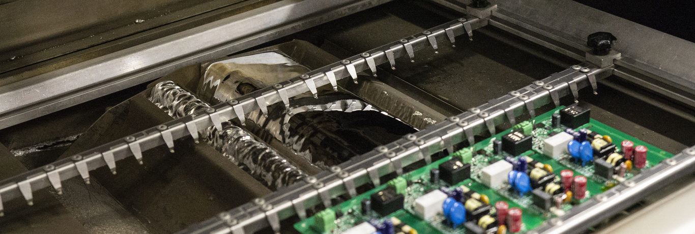
A typical wave solder machine consists of multiple functional modules working in sequence: preheating, fluxing, the solder wave itself, and post-solder cooling. These stages are integrated through a conveyor system that transports the PCB through the process at a controlled speed. The most critical section is the solder wave, created by pumping liquid solder through a shaped nozzle, forming a standing wave that makes uniform contact with the side of the PCB containing the component leads.
The soldering machine is engineered to maintain specific process parameters such as solder temperature, wave height, and contact time, which are essential for achieving reliable solder joints. Variations in these settings can result in solder defects such as bridging, icicling, or insufficient wetting. Therefore, advanced wave soldering systems often feature automated control loops and real-time monitoring to maintain consistency and mitigate soldering problems.
Additionally, the integration of nitrogen environments within modern wave solder machines reduces oxidation and improves the wettability of the solder, contributing to more efficient soldering results and reducing rework rates.
The selection of solder alloy is a critical aspect of the wave soldering process, directly affecting the reliability, conductivity, and mechanical strength of the final solder joints. Traditional wave soldering systems used lead-based alloys such as Sn63-Pb37 due to their low melting points and excellent flow characteristics. However, with the adoption of environmental directives like RoHS, lead-free solder alloys typically based on tin-silver-copper (SAC) compositions have become the standard in PCB assembly.
Each alloy presents different challenges in terms of melting behavior, oxidation tendencies, and compatibility with flux formulations. For example, lead-free solder generally requires higher process temperatures and may exhibit increased dross formation, which must be managed carefully to maintain efficient soldering.
In selective applications, especially where selective wave soldering machines are used, the choice of solder is further influenced by the localized nature of the solder wave, requiring alloys that support precise deposition and strong soldering quality under constrained thermal profiles.
The solder wave height is a pivotal parameter in determining the success of a wave soldering process. It defines the degree of contact with the solder, influencing how well the through-hole leads are wetted and how much solder is deposited around each pin. Both too low and too high a wave height can compromise solder joint integrity, leading to defects that affect electrical performance and mechanical durability.
Consistency in wave height is particularly important in high-density boards, where uneven solder distribution can cause bridging between adjacent pads or leave some joints underfilled. For this reason, wave soldering machines are equipped with precise control mechanisms to regulate the height of the solder wave and ensure optimal contact angles across all lead geometries.
Modern soldering machines allow operators to fine-tune the solder wave height using software-based controls and mechanical adjustments. This tuning is based on parameters such as board thickness, component lead length, and the orientation of THT components. Adjustments are typically made by modifying the pump speed, altering the nozzle configuration, or changing the machine use settings in real time.
When working with selective wave techniques, these adjustments become even more critical. The fill in mini wave soldering demands a high degree of precision in wave height to ensure adequate penetration into the THT holes without damaging nearby SMD components or causing thermal stress.
Temperature control within the soldering system is fundamental to achieving consistent soldering results. The solder wave must be maintained within a narrow thermal window usually around 250°C for lead-free alloys to ensure proper wetting and flow characteristics. Deviations from this window can result in incomplete hole fill, poor adhesion, or thermal damage to the board.
Flow dynamics are equally essential. The movement of the liquid solder within the solder wave must be laminar and uninterrupted to avoid turbulence that can trap air bubbles or cause spattering. These flow characteristics are managed by the design of the nozzle and the pump system, both of which must be aligned with the specific design rules of the board under assembly.
Prior to entering the solder wave, the PCB undergoes a preheat phase, which prepares both the board and the flux for optimal performance. The preheat section of the wave soldering system gradually raises the temperature of the circuit board to reduce thermal shock, activate the flux, and promote efficient outgassing of any volatile compounds. This stage is crucial for minimizing solder defects and ensuring proper wetting of the joints.
Flux plays an indispensable role in the solder process, acting as a chemical agent that removes oxides from metal surfaces and facilitates the bonding of solder to component leads and pads. It must be carefully selected based on the solder alloy, board materials, and process parameters.
The preheat zones are typically divided into several stages, each with independently controlled heating elements. These zones are designed to achieve a gradual thermal ramp-up, which is critical for preventing thermal stress on the board and components. A well-optimized preheat profile helps the flux activate fully, enhances solderability, and contributes directly to the formation of strong and reliable solder joints.
An improperly controlled preheating and soldering profile can result in poor flux activation, leading to oxidation and increased occurrence of soldering problems. Therefore, maintaining the correct thermal energy balance across preheat and soldering stages is key to ensuring consistent soldering quality in both traditional and selective wave soldering processes.
Selective wave soldering is a refined evolution of traditional wave soldering, developed to address the increasingly complex nature of PCB designs that incorporate both THT components and SMD elements. In contrast to the full-board exposure used in conventional processes, selective techniques apply solder only to designated areas of the PCB, allowing precise and localized THT soldering without disturbing adjacent components sensitive to heat.
This special form of wave soldering is particularly beneficial in mixed-technology assemblies where reflow is used for SMDs, and only specific zones require THT connections. In such cases, using traditional wave soldering would risk overheating sensitive components or reflowing previously soldered parts. Thus, selective wave soldering enables manufacturers to isolate through-hole technology from heat-sensitive regions while maintaining the mechanical and electrical advantages of robust THT solder joints.
The method is typically applied in scenarios where design constraints, thermal limitations, or selective component integration necessitate high-precision soldering methods. It is also favored in industries requiring advanced electronics manufacturing standards, such as medical, military, and aerospace sectors.
A selective wave soldering machine integrates several subsystems that operate in a tightly controlled sequence to ensure accuracy, efficiency, and repeatability. Unlike standard wave solder machines, where the entire PCB is exposed to a solder wave, selective systems use compact, movable nozzles to deliver liquid solder directly to the target areas. The board itself remains stationary or moves along a precision-guided conveyor that positions it relative to the soldering module.
These machines are composed of several critical units: the spray fluxer, preheat station, solder pot with precision nozzles, and often a nitrogen enclosure to reduce oxidation and improve soldering quality. The high degree of configurability allows them to accommodate various PCB layouts, especially those with dense or asymmetric component placements that would be incompatible with a full solder wave.
This technology enables high-accuracy soldering with minimal risk to the surrounding SMD components, offering both thermal and spatial control that is unachievable in conventional setups.
The nozzle is the heart of any selective wave soldering machine. It directs the solder wave with pinpoint accuracy, ensuring that THT holes receive the appropriate volume and contact time with liquid solder. Depending on the soldering method, the nozzle may be programmed to follow complex paths, pause over specific joints, or adjust flow rates dynamically based on feedback from sensors.
Precision in solder flow is essential, as inconsistent delivery can lead to insufficient hole fill, cold joints, or bridging. The design and calibration of the nozzle, along with real-time adjustment algorithms, allow for stable solder wave height and accurate thermal delivery. This ensures optimal wetting, especially important for fill in mini wave soldering operations.
Moreover, the machine use of adaptive motion control systems enables efficient transition between different THT patterns, significantly improving production flexibility without compromising soldering results.
In selective systems, fluxing is usually applied via a spray fluxer, which accurately deposits flux only on the pads or THT holes to be soldered. The precision of this application helps prevent contamination of adjacent SMD components and minimizes residue formation.
Effective flux application is followed by controlled preheat stages, which are crucial to activating the flux and ensuring uniform thermal profiles. The preheating and soldering sequence must be tuned precisely to allow sufficient outgassing of the flux without exceeding thermal limits for sensitive areas. Well-designed preheat zones enhance solder wetting and minimize thermal stress, improving the overall soldering quality.
These preparatory stages are not mere supplements but integral elements of the solder process, influencing everything from solder joint reliability to long-term product durability. Their integration with the core soldering module ensures seamless control and reproducibility.
The main distinction between selective wave soldering and conventional wave soldering lies in the extent of the board exposed to molten solder. While the latter submerges the entire underside of a PCB, selective methods target only specific locations using localized solder waves.
In terms of design for manufacturing, selective techniques offer significant advantages for complex boards that include tightly packed through-hole and surface mount elements. With a wave soldering process that can be localized, the thermal stress imposed on the board is significantly reduced, and the manufacturing processes become more adaptable to product variation and design complexity.
From a dimensioning on manufacturability in selective perspective, selective systems allow for finer control over THT-hole dimensioning on manufacturability, as only predefined areas are subject to thermal energy and solder contact. This results in fewer restrictions during the PCB design phase and opens opportunities for more intricate routing and placement strategies.
While conventional wave soldering remains faster and more economical for high-volume production runs involving simple through-hole boards, selective wave soldering is more suitable for assemblies with diverse components and design intricacies. Although the initial investment in a selective soldering machine may be higher, the long-term benefits such as reduced rework, lower defect rates, and compatibility with modern smt machines justify its use in many applications.
Selective soldering also results in better process robustness due to its adaptability. It accommodates dynamic production schedules and variable board designs without compromising soldering is used performance. This flexibility is crucial in industries where customization and reliability are paramount.
Ultimately, the choice between the two methods depends on the specific demands of the electronics manufacturing process, the complexity of the circuit board, and the balance between speed, cost, and precision. As selective wave soldering continues to evolve, its role in enabling complex PCB assembly with mixed-technology configurations is set to expand further.
The development of high-performance PCB assemblies incorporating THT components requires a thorough understanding of both wave solder and selective solder process constraints. As THT wave soldering becomes increasingly integrated into mixed-technology boards, designers must prioritize manufacturability at every stage, aligning PCB layout, component placement, and pad geometries with the capabilities of modern soldering systems.
Wave soldering is an efficient method for mass-producing through-hole connections, but its success hinges on precise control of process variables that are heavily influenced by the underlying board design. When transitioning to selective wave soldering, the importance of design increases, as localized heating and solder delivery magnify the impact of spacing, thermal mass, and accessibility.
Effective pad design is foundational to reliable THT soldering. Pads must be dimensioned to ensure full wetting during the soldering process while minimizing the risk of bridging or tombstoning, particularly near SMD components. The spacing between through-hole leads must accommodate the tolerances of the soldering machine’s motion system and nozzle diameter, especially in selective wave applications.
Close attention to pad-to-hole alignment is essential when considering dip soldering or selective soldering systems, as misalignment can cause inconsistent solder flow or partial wetting. Designers must also consider the orientation of component leads in relation to the direction of the solder wave to avoid shadowing and insufficient contact. This factor was historically addressed when wave soldering was invented to meet the demands of automated PCB assembly, and it remains just as critical in today's high-precision environments.
The THT-hole dimensioning on manufacturability is a nuanced discipline that balances mechanical, thermal, and process requirements. Holes must be large enough to facilitate solder flow but not so oversized that they compromise mechanical retention or allow for excessive solder usage. Proper ratio between lead diameter and hole size directly impacts hole fill in mini wave processes, especially in selective wave soldering.
In selective environments, these tolerances become tighter due to the localized and directed nature of the solder wave. The interaction between flux, preheat, and wave height becomes highly dependent on these dimensions. Therefore, incorporating design rules that reflect real-world machine use constraints is vital to achieving consistent soldering results without costly rework or defects.
The surface of the circuit board should also be designed to ensure unobstructed access for the soldering nozzle, with component bodies or shielding elements positioned in a way that does not block the solder wave or prevent effective thermal energy transfer.
Reliable soldering begins with solderability, which is influenced by the metallurgical compatibility of component terminations and PCB finishes with the selected solder alloy. Surface finishes such as HASL, ENIG, or OSP interact differently with common solder types and require tailored flux formulations to ensure effective wetting during the wave soldering process.
Solderability is especially critical in selective wave soldering, where insufficient flux activation or poor wetting can result in cold joints or incomplete through-hole filling. The transition from traditional leaded to lead-free solder compounds the challenge, as higher process temperatures and oxidation risks demand rigorous attention to material compatibility.
The selection of the solder alloy plays a central role in both process reliability and product performance. Lead-free alloys, such as SAC305, are now industry standards due to regulatory compliance, but they introduce new complexities in THT soldering, particularly in selective processes where the soldering method must account for narrower thermal profiles and greater sensitivity to oxidation.
Component lead materials must be compatible with the chosen alloy to ensure proper intermetallic formation and long-term reliability. The solder joint formation must be stable under both electrical and mechanical stresses, especially in high-reliability applications like power electronics.
Furthermore, the board substrate material and copper thickness impact thermal energy absorption and dissipation during the preheat and soldering stages. These factors must be considered in both process design and PCB design, particularly when optimizing for selective techniques using compact nozzles and localized solder wave height control.
The effectiveness of a wave soldering system whether traditional or selective depends heavily on its alignment with the PCB layout and process expectations. The design phase must consider all elements of the solder process, from flux chemistry to preheat temperature gradients and final soldering parameters.
Advanced smt machines and selective wave soldering machines offer fine control over solder application, allowing for precise process tuning. However, they also require higher design discipline to ensure compatibility. For example, insufficient spacing between THT pads and SMDs may prevent the nozzle from accessing the joint or cause unintended heating.
To fully leverage the capabilities of a selective wave soldering machine, PCB layouts must reflect the physical and thermal constraints of the process. This includes ensuring adequate conveyor clearance, predictable heat flow across copper planes, and accessible geometries for the soldering nozzle.
Designers should also implement thermal simulations during layout to predict how the board will respond to localized heating. These insights enable engineers to fine-tune preheating and soldering profiles, optimize wave height, and avoid warping or delamination.
Ultimately, wave soldering is used not just as a means of connection, but as a critical contributor to product reliability and performance. Its application in the selective domain depends as much on PCB design as on machine use, underscoring the necessity of early, cross-disciplinary collaboration in the product development cycle.
The verification of THT solder joints is a fundamental element of quality assurance in electronics manufacturing, especially when employing complex processes such as wave soldering and selective wave soldering. As the physical and electrical integrity of every solder joint directly affects the reliability of the final product, rigorous inspection methodologies must be implemented across all stages of PCB assembly.
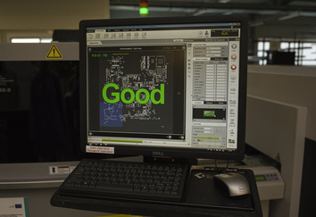
Post-solder inspection focuses not only on detecting defects but also on evaluating soldering quality including hole fill, wetting angles, and the uniformity of the solder fillet. These indicators reflect the efficacy of the solder process, the compatibility of materials, and the performance of the soldering system.
Visual inspection remains a baseline technique in evaluating THT solder quality, particularly for identifying macroscopic issues such as cold joints, bridges, and insufficient solder fill. However, its subjective nature and limited accessibility in densely populated boards necessitate the use of advanced tools.
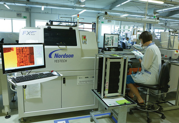
Automated Optical Inspection (AOI) is widely used to assess surface-level soldering results with high repeatability. AOI systems detect deviations in pad coverage, fillet shape, and component alignment, providing immediate feedback on soldering problems.
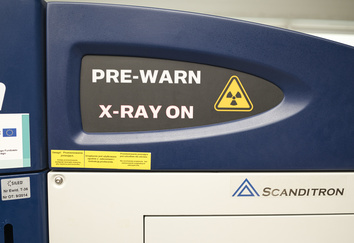
For defects obscured by components or located within through-hole structures, X-ray inspection offers a powerful solution. This non-destructive technique enables internal examination of THT and SMD joints, ensuring compliance with quality standards even in concealed areas. In selective soldering systems, X-ray imaging is particularly valuable for validating fill in mini wave soldering, where precise solder wave application must be confirmed.
Despite the maturity of the wave soldering process, a range of defects can still occur due to variability in board design, soldering method, component geometry, and process parameters. Understanding the root causes and implementing robust countermeasures are essential steps toward achieving high-yield production.
The most common soldering problems include:
Insufficient hole fill – often caused by improper flux activation, low solder wave height, or short contact time.
Solder bridges – usually a result of excessive solder, narrow pad spacing, or uneven wave height across the board width.
Cold joints – typically due to poor thermal contact or contaminated surfaces, indicating issues with preheat or material compatibility.
Icicling and webbing – can occur when wave soldering is used with incompatible geometries or when the solder lacks sufficient surface tension control.
Preventing these defects involves a combination of well-executed PCB design, optimal machine use, and continuous monitoring of process variables. Proper design rules, including lead-to-hole ratio, component orientation, and pad layout, reduce the risk of solder bridging and voids. Ensuring that the preheat profile aligns with the thermal energy demands of the assembly enhances flux activation and wetting behavior.
From the equipment perspective, maintaining consistent solder wave height is critical, especially in selective wave soldering, where even minor deviations can impact the precision of solder deposition. Regular calibration of the nozzle system, combined with real-time feedback from vision or temperature sensors, mitigates variability across production lots.
Furthermore, controlling the atmosphere around the soldering machine, particularly with nitrogen inerting, helps reduce oxidation and improves the overall wetting performance of the liquid solder, resulting in more uniform solder joints.
Ensuring repeatability and process robustness in wave soldering and selective wave soldering machines requires a sophisticated control framework. Modern systems are equipped with advanced software tools and real-time data acquisition modules that track key parameters throughout the entire soldering process.
These control systems enable predictive maintenance, process traceability, and rapid diagnostics in case of anomalies. Integration with MES (Manufacturing Execution Systems) platforms also enhances production transparency and compliance with quality standards.
Among the most critical parameters in both conventional and selective processes are solder wave height and temperature stability. Variations in wave height can lead to inconsistent contact with THT leads, directly affecting solder joint formation. Similarly, thermal deviations can impact flux activation, wetting behavior, and the integrity of component packages.
Monitoring tools, including laser sensors and thermocouples, provide precise measurements of solder wave dimensions and heat distribution. These measurements are used to make real-time adjustments to pump speeds, nozzle positioning, and preheat settings.
A well-maintained soldering system must ensure that all thermal and mechanical parameters remain within tightly controlled tolerances. By stabilizing these variables, manufacturers not only reduce the likelihood of defects but also reinforce the efficient soldering capability that makes wave soldering indispensable in high-reliability circuit board production.
The evolution of selective wave soldering has enabled its widespread adoption across a variety of industries that demand high reliability, precision, and component density. This soldering method is particularly advantageous in sectors where the convergence of THT components with sensitive SMD parts is common and where conventional wave soldering is used cannot guarantee thermal isolation or placement accuracy.
In contemporary electronics manufacturing, selective wave soldering offers the flexibility to accommodate custom configurations, comply with stringent safety regulations, and deliver consistent soldering quality at scale. Its selective nature ensures thermal protection of delicate components while maintaining robust solder joints in high-power or mission-critical applications.
In the automotive sector, electronic control units (ECUs), power distribution modules, and infotainment systems frequently incorporate high-current THT connections alongside dense arrays of SMD parts. Selective wave soldering enables precise joining of these components without reflowing nearby thermally sensitive parts. Additionally, the soldering process must meet rigorous durability standards, including resistance to vibration, temperature cycling, and humidity exposure conditions under which efficient soldering and proper hole fill in mini wave techniques are critical.
The aerospace industry presents even greater challenges, where component reliability and traceability are paramount. Avionics systems and navigation modules rely on secure THT solder joints, often on multilayer PCBs with complex internal copper planes. In such assemblies, selective soldering systems allow designers to implement redundant electrical paths without sacrificing thermal control during preheat and solder wave stages.
Medical devices such as defibrillators, patient monitors, and diagnostic imaging equipment must meet strict regulatory and performance benchmarks. Here, selective soldering ensures both compact form factors and robust electrical integrity, particularly for connectors and power entry modules that necessitate through-hole technology.
Across all these domains, the integration of selective wave soldering machines with automated inspection systems and traceable data logging has become standard, supporting continuous improvement and compliance with international quality systems.
Even in highly optimized production environments, soldering problems can arise due to the inherent complexity of the wave soldering process. A systematic approach to troubleshooting is essential to identify the root cause of failures and to implement lasting corrective actions. Problems may originate from various sources, typically falling into three categories: design, process, or machine parameters.
A structured diagnostic strategy considers all aspects of the system from PCB design and component geometry to soldering system configuration and environmental factors such as nitrogen flow or ambient humidity. Understanding the interdependencies between these variables enables effective process stabilization and prevents recurring defects.
Design-related issues often stem from improper dimensioning on manufacturability in selective environments. For instance, insufficient spacing between THT holes and adjacent SMDs can prevent adequate nozzle access or cause uneven thermal energy distribution. Boards with excessive copper mass or poor thermal symmetry may experience localized overheating or incomplete solder wetting, especially during selective wave operations.
Process-related failures typically involve deviations in flux application, preheat profiles, or solder wave height. If flux is insufficient or unevenly distributed, oxides may remain on contact surfaces, resulting in poor solderability or non-wetted joints. Similarly, under- or over-heating during preheating and soldering can lead to thermal damage or improper solder joint formation.
Machine-related causes are frequently associated with pump malfunctions, inaccurate conveyor calibration, or nozzle wear. A misaligned soldering module or fluctuating solder temperature can produce inconsistent soldering results, even when other parameters appear correct. In such cases, regular preventive maintenance and automated monitoring are vital to ensure better process robustness.
Ultimately, effective troubleshooting requires a holistic view of the manufacturing processes, supported by cross-functional collaboration between design engineers, process technicians, and equipment specialists. This multidisciplinary approach ensures that failures are not only corrected but prevented through ongoing optimization and feedback into the design cycle.
As the demands of the electronics industry grow in complexity and scale, the future of THT soldering lies in increased automation and tighter integration of hardware and software systems. Modern wave soldering systems are transitioning toward intelligent, data-driven platforms that utilize real-time monitoring, closed-loop control, and predictive maintenance strategies to enhance throughput, consistency, and yield.
Emerging soldering machines are no longer isolated tools but interconnected modules within larger smart factory frameworks. These machines feature automatic adjustments for solder wave height, adaptive nozzle paths in selective wave soldering, and integrated inspection cameras capable of detecting anomalies as they occur.
Incorporating machine learning into wave solder environments allows process optimization based on historical data, enabling continuous improvements and reduction of human intervention. Combined with advanced smt machines, this trend promises to bridge THT and SMT technologies seamlessly in hybrid PCB assemblies, improving efficiency across all layers of production.
Such automation ensures better alignment with design and process parameters, minimizing downtime, rework, and defect rates, and allowing manufacturers to scale operations without sacrificing soldering quality.
The movement toward sustainability and environmental compliance is shaping the future of PCB assembly, particularly in relation to materials used in the soldering process. One of the most significant shifts has been the transition from leaded to lead-free solder alloys, a change driven by global regulations such as RoHS and REACH.
While lead-free solder presents challenges including higher melting points, increased oxidation, and altered wetting behavior ongoing research is addressing these issues by developing more robust fluxes and improving thermal energy profiles during preheating and soldering.
Future wave soldering systems are expected to incorporate more energy-efficient designs, with enhanced thermal management systems and the ability to recycle and refine excess liquid solder. Additionally, there is a growing emphasis on reducing waste from flux residues and minimizing the use of harmful chemicals in spray fluxers.
The push for greener production also extends to board design, where surface of the circuit board materials are being selected not only for performance but also for recyclability and lower environmental impact. This holistic approach ensures that sustainability is embedded not only in soldering methods but across the entire electronics manufacturing ecosystem.
As electronic devices continue to miniaturize while increasing in functionality, high-density PCB design is becoming the new standard. In this landscape, selective wave soldering plays a critical role, providing a targeted solution for THT components within densely populated boards dominated by SMDs.
The future of selective wave soldering is characterized by higher precision, multi-nozzle configurations, and deeper integration with design automation tools. Engineers are now able to simulate fill in mini wave soldering, thermal gradients, and solder joint behavior in digital environments before physical production begins.
New innovations in selective soldering systems include ultra-fine nozzle tips for micro-connector applications, dynamic path optimization based on real-time board analysis, and integration with 3D inspection systems that confirm soldering results layer by layer.
As wave soldering is a special yet increasingly essential part of hybrid PCB design, its evolution is closely tied to advances in design automation and design for manufacturing principles. The collaboration between mechanical designers, process engineers, and software developers will be essential in crafting next-generation soldering modules capable of meeting the stringent requirements of aerospace, medical, and high-performance computing systems.
The path forward merges the legacy robustness of through-hole technology with the agility of modern digital manufacturing securing THT wave soldering a central place in the future of high-reliability, high-density electronics production.
The continuous advancement of electronic assembly technologies has reaffirmed the relevance and adaptability of THT soldering, particularly when integrated with wave soldering and selective wave soldering systems. While surface mount technology dominates modern designs, through-hole technology remains indispensable for applications demanding mechanical durability, power integrity, and thermal resilience.
This article has comprehensively explored the principles, machinery, and techniques behind wave soldering and its selective counterpart, emphasizing the interplay between design for manufacturability, soldering system configuration, and process control. The analysis of solder joint inspection methods, defect prevention, and the influence of PCB design rules provides a practical framework for improving both production quality and long-term reliability.
Looking ahead, the integration of automation, data-driven control, and sustainable practices will shape the future of THT soldering and wave soldering systems, aligning technical innovation with ecological and industrial needs. In this dynamic landscape, achieving excellence requires a collaborative approach that spans engineering disciplines, combines robust design strategies, and leverages the full potential of modern soldering technologies.