SMT Assembly: Surface mount circuit design, PCB assembly techniques, and SMT line optimization
SMT assembly refers to the method of mounting electronic components directly onto the surface of a printed circuit board using Surface Mount Technology (SMT). This contrasts sharply with through-hole technology, where component leads are inserted through pre-drilled holes. SMT enables higher component density, more compact circuit designs, and faster, more reliable manufacturing. By eliminating the need for holes and leveraging automation, SMT facilitates the efficient placement of components such as capacitors, resistors, and integrated circuits.
A typical SMT assembly process involves several precisely controlled stages: applying solder paste using a stencil, placing components with a pick-and-place system, and forming strong solder joints through a thermal reflow cycle. This streamlined assembly process reduces the footprint of electronic products while maintaining or improving performance, particularly in high-frequency applications. SMT has become integral to the electronics assembly industry, playing a foundational role in modern PCB assembly.
The shift from through-hole assembly to surface mount assembly began in the late 20th century as electronic devices demanded greater miniaturization and functionality. The development of SMD components, combined with improved PCB design tools and automated assembly equipment, allowed engineers to implement more complex circuit boards in smaller packages. As the production process matured, manufacturers transitioned from manual to automated solutions, including the introduction of pick-and-place machines and reflow ovens for enhanced throughput and consistency.
This technological advancement has led to a significant transformation in PCB assembly service practices. Early assembly methods were often labor-intensive and prone to variation. In contrast, today's SMT systems deliver exceptional accuracy and repeatability, supporting the creation of intricate multilayer boards with micro-scale features and extremely fine lead pitch. The shift also enabled the electronics sector to respond rapidly to consumer demand for lighter, thinner, and more energy-efficient devices.
The advantages of surface mount technology are numerous and continue to drive its dominance in the field of electronic manufacturing services. One of the primary benefits is miniaturization, which allows more functionality to be packed into a smaller form factor without compromising performance. Additionally, surface mount components can be mounted on both sides of a printed circuit board, further enhancing space utilization and design flexibility.
From a manufacturing standpoint, SMT enables faster production cycles through a fully automated smt line, reducing labor cost while improving yield. The use of lead-free solder in compliance with environmental standards, combined with convection heating in reflow soldering, ensures strong mechanical and electrical connections. These solder joints are critical for long-term reliability, particularly in mission-critical applications where failure is not an option.
Another critical aspect is defect reduction. Advanced inspection techniques, including automated optical inspection (AOI) and in-circuit functional testing, detect issues such as missing or misaligned components early in the production line, thereby increasing product quality and consistency. Additionally, SMT supports easy rework and repair using specialized equipment such as a rework station, allowing precise adjustments and corrections onto the PCB without damaging adjacent structures.
In conclusion, SMT represents a convergence of material science, mechanical engineering, and automation. It enables the realization of high-speed, low-power, and reliable electronic systems that are central to modern life. As we move into the next section, the focus will shift toward the specific stages of the SMT assembly process, offering a detailed view of how theory meets practice in today's advanced manufacturing environments.
The SMT assembly process is a highly controlled and sequential series of operations that ensure electronic components are accurately placed and reliably soldered onto a printed circuit board. This manufacturing process is designed for precision, scalability, and repeatability, forming the backbone of modern PCB assembly. It begins with the preparation of the board and ends with testing and inspection to ensure functional compliance and mechanical stability.
The process flow starts with board cleaning and preparation, followed by the application of solder paste to the pads using a precision-engineered stencil. This paste acts both as an adhesive and as a soldering medium. The board then moves to the pick-and-place stage, where machines place each SMD component onto the PCB with micrometer-level accuracy. Once all components are in position, the board enters a reflow oven, where heat causes the solder to melt and form solder joints that secure the parts to the board. The thermal profile must be carefully controlled to ensure proper reflow while avoiding thermal damage or component misalignment.
After soldering, the board is cooled and sent for inspection. This includes automated optical inspection (AOI) and in-circuit tests that verify correct placement, polarity, and connectivity. In cases where rework is necessary, a rework station allows operators to remove or replace components without compromising the board's integrity. Once validated, the board can proceed to packaging or further system-level integration. Every step in the process requires precise environmental controls and high standards to maintain the reliability of the final product.
This structured flow is crucial not only for high-volume manufacturing but also for prototype and prototype assembly, where quick iterations and accuracy are essential. Whether the objective is rapid prototyping or large-scale production, understanding this process flow is vital for successful electronics assembly.
Each step in surface mount assembly contributes to the integrity and performance of the final circuit. The process begins with board preparation, where solder mask is applied during fabrication to protect areas of the board not intended for soldering. This mask defines the regions where solder paste will later be applied. Once the board is ready, a stencil is aligned over it, and a controlled amount of paste is deposited on the exposed pads using a squeegee system. The uniformity and placement of the paste are critical for achieving reliable solder joints during reflow.
Following paste application, the component placement stage begins. A high-speed pick-and-place machine selects components from reels or trays and positions them with exceptional precision. This includes a wide range of assembly elements, from resistors and capacitors to microprocessors and other complex integrated circuits. The system uses vision alignment tools to ensure each component lands exactly on its intended pad, accommodating various geometries and lead pitch specifications.
The placed board then enters the reflow soldering phase. Here, the board passes through a reflow oven, where temperatures are carefully ramped up and down in accordance with a thermal profile optimized for the materials used. The hot air or convection heating ensures the solder reflows and forms metallurgical bonds between component leads and board pads. Properly executed, this stage guarantees both electrical connectivity and mechanical strength. Overheating or underheating at this stage can lead to defects like solder balls, tombstoning, or cold joints.
After soldering, the board undergoes inspection. AOI systems scan the surface to detect missing or misaligned components, insufficient solder, or bridging. These systems use advanced imaging and pattern recognition algorithms to catch flaws invisible to the naked eye. In mission-critical applications, additional functional testing and in-circuit verification are performed to confirm the board behaves as expected.
In some cases, through-hole components are still necessary, often added after SMT processing. This hybrid technique, known as mixed technology, combines the benefits of surface mount and through-hole assembly, especially when handling components that require mechanical robustness or carry high currents. When such components are involved, additional soldering steps, often using wave or selective soldering, are introduced into the assembly line.
Finally, the completed board may move on to coating, marking, or housing integration, depending on the end-use. At this stage, if required, the PCB assembly service provider will integrate the board into a final system or deliver it for further customer testing. Regardless of the volume or application, understanding and controlling each stage of this process ensures successful outcomes in both PCB manufacturing and final product performance.
The application of solder paste is one of the most critical stages in the SMT assembly process, as it directly influences the formation and quality of solder joints, which in turn determine the electrical and mechanical reliability of the assembled board. Solder paste is a composite material consisting of fine metal particles—typically tin, silver, and copper—in a flux matrix that facilitates metal wetting and oxidation removal during reflow. Its purpose is twofold: to temporarily hold components in place and to provide the necessary metallic connection during the soldering process.
In the context of PCB assembly, the uniformity and placement accuracy of solder paste are fundamental. Any deviation in paste volume, distribution, or viscosity can lead to severe defects such as open joints, bridging, or the formation of undesirable solder balls. As modern surface mount components continue to decrease in size while lead pitch tightens, the demand for precise paste application increases significantly. This makes control of paste composition, particle size, and stencil aperture geometry crucial to the overall performance of the PCB assembly process.
Beyond placement, the thermal behavior of solder paste during reflow also requires attention. The paste must withstand board handling and component placement, yet melt and flow adequately during thermal cycling in a reflow oven. Its thermal profile must align with the characteristics of both the paste alloy and the components themselves to ensure a reliable solder joint. Any discrepancy—such as excessive voiding, incomplete wetting, or flux residue—can compromise the circuit integrity, particularly in high-speed or high-reliability applications.
In environments where lead-free processing is mandated, the behavior of solder paste changes, especially in terms of melting point and oxidation characteristics. These factors influence the choice of reflow parameters and even the selection of paste type. Flux chemistry plays a significant role here, as it not only facilitates oxide removal during soldering but also impacts the cleaning requirements post-reflow, especially in no-clean or low-residue applications.
Ultimately, solder paste is far more than a binding agent. It is a key enabler of high-performance electronics assembly, and its role must be rigorously optimized and controlled to meet the growing challenges of component miniaturization, high-speed design, and the increasing demands of electronic manufacturing services.
The stencil serves as a mechanical mask used to accurately apply solder paste to designated pads on the surface of a printed circuit board. It is typically fabricated from stainless steel and is produced using laser cutting or chemical etching methods. The precise design of a stencil—including aperture size, shape, and thickness—determines how much paste is deposited onto each pad, directly affecting the quality of solder joints and overall assembly integrity.
The aperture design of the stencil must correspond to the PCB design and component footprint. Inadequate or excessive solder can cause bridging, tombstoning, or insufficient connections. Engineers must carefully balance aperture area ratio, aspect ratio, and paste release characteristics to ensure a clean and complete transfer. As SMD components become smaller and more densely packed, stencil optimization becomes increasingly critical to accommodate narrow spacing and tight lead pitch.
Modern PCB manufacturing often employs step stencils or multi-level stencils to manage varying paste volumes across a single board. These adaptations are especially important when both fine-pitch and large passive components appear in the same layout. In such scenarios, a single uniform thickness would not yield ideal results. Instead, step-down areas for small components and step-up regions for larger pads ensure that each circuit location receives the optimal paste volume for effective reflow.
Stencil alignment is another essential consideration. High-precision printing systems use fiducial marks on both the stencil and the PCB to achieve micron-level alignment. Misalignment at this stage may result in paste being deposited outside the intended pad areas, leading to missing or misaligned components during component placement or weak solder joints after reflow. Some manufacturers also employ solder paste inspection systems (SPI) to verify paste volume, coverage, and location before the board progresses to the next stage.
Proper stencil maintenance is vital as well. Residue buildup and paste drying inside apertures can lead to inconsistent deposition, which becomes increasingly problematic in high-volume production or fine-pitch applications. Cleaning routines—whether manual or automated—must be incorporated into the workflow to preserve stencil functionality and ensure consistent print quality.
In summary, the stencil is not a passive tool but a high-precision component in the broader assembly process. Its role in enabling uniform, accurate solder paste deposition makes it an essential element of high-yield, defect-free surface mount technology operations. As automation and miniaturization continue to define the trajectory of electronics, the engineering behind stencil design and application will only grow in significance.
The success of any SMT assembly begins with a precise understanding of surface mount components and their characteristics. These components, commonly referred to as SMDs, include a wide variety of package types such as chip resistors, ceramic capacitors, transistors, diodes, and complex integrated circuits. Unlike components used in through-hole assembly, SMDs are designed without protruding leads, often utilizing metallized terminals, pads, or ball-grid arrays for electrical connection. Their compact dimensions support high-density circuit layouts essential to contemporary printed circuit board designs.
Proper handling of SMT components is crucial due to their miniaturized form and susceptibility to damage. Electrostatic discharge (ESD) sensitivity is a significant concern, particularly with active devices like microcontrollers and memory chips. Additionally, mechanical stress during transport or feeding can result in cracks or microfractures, which may not be visually apparent but can compromise solder joint integrity during reflow. Humidity control is also essential; components exposed to moisture can experience delamination or popcorning during reflow soldering due to rapid internal vaporization.
Storage conditions must comply with strict moisture sensitivity level (MSL) guidelines, and the use of humidity-controlled environments or dry cabinets is common practice in advanced electronics assembly operations. Proper packaging formats—such as tape-and-reel, trays, or tubes—facilitate seamless integration with pick-and-place machines, minimizing manual intervention and the risk of contamination or misplacement. With increasing use of leadless and ultra-miniature packages, the margin for handling error has become exceptionally narrow, reinforcing the need for precise procedural control at every stage of SMT operations.
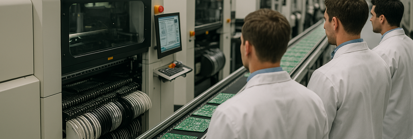
Component placement on the SMT line is a core operation that defines both the speed and precision of the overall assembly process. At this stage, a programmed pick-and-place system retrieves each electronic component from its feeder and positions it accurately onto the PCB at designated coordinates. The placement is not only about location but also orientation, alignment, and contact pressure—all of which influence final solder reliability and performance.
Early generations of component placement equipment were limited by mechanical tolerances and vision systems. However, modern machines have evolved to incorporate advanced imaging, laser centering, and real-time correction algorithms that can achieve placement accuracy within a few micrometers. These systems support a wide range of assembly requirements, from low-volume prototype runs to high-speed production involving thousands of placements per hour.
Components are identified by part numbers and matched with corresponding footprint libraries generated during the PCB design phase. Fiducial marks on the board provide positional references that allow the machine to compensate for board misalignment or warping. The smt process also includes precise nozzle selection for each component type, ensuring that even delicate or asymmetrical parts are picked and placed without damage.
One of the challenges in this phase is achieving consistent placement force, particularly when dealing with varying package heights and pad structures. An inadequate contact between the component and the solder paste can result in poor solder joint formation during reflow, while excessive force can smear the paste or crack fragile components. To address this, many machines now incorporate force sensors and vision alignment at multiple stages—before, during, and after placement.
Modern SMT lines may also include inline component verification, which checks for correct part numbers and orientation before placement. This added layer of control helps prevent errors such as rotated or flipped components, which are among the most common defects in dense circuit boards. By ensuring that each part is accurately placed under optimal conditions, this stage establishes the physical and electrical foundation for successful PCB assembly.
Automation lies at the heart of high-performance SMT operations. The ability to place components with extreme accuracy and repeatability has enabled manufacturers to meet the growing demands of complex circuit design, compact form factors, and accelerated production schedules. Today’s advanced pick-and-place machines are capable of processing tens of thousands of components per hour while maintaining high first-pass yield and minimal defect rates.
The term accuracy and repeatability refers to the machine’s ability to consistently position components in exactly the same place across many boards and production runs. These characteristics are influenced by several factors, including the machine’s mechanical stability, vision system resolution, calibration procedures, and even environmental variables such as temperature and vibration. The integration of real-time feedback and closed-loop control systems has greatly improved performance in these areas.
Placement accuracy is especially critical for devices with fine lead pitch, such as QFNs or BGAs, where a slight misalignment can lead to shorts or opens that may not be easily visible. In such cases, even a deviation of a few microns can disrupt the soldering process, leading to weak solder joints, intermittent connectivity, or long-term reliability issues. As component dimensions shrink and board complexity increases, the tolerance for placement error approaches zero.
To ensure optimal results, production line calibration and maintenance must be routinely performed. This includes the alignment of feeders, checking for nozzle wear, validating vision alignment, and verifying software libraries against current component datasets. Additionally, simulation and off-line programming tools allow engineers to pre-validate placement sequences, reducing changeover time and minimizing errors during high-mix production runs.
In conclusion, the success of SMT assembly is deeply tied to the capabilities of automated component placement systems. These machines must manage a complex interplay of mechanical precision, imaging, software intelligence, and environmental stability to meet the challenges of modern PCB assembly. With the growing sophistication of electronic products, the pressure on placement technologies to deliver error-free results at scale will only continue to rise.
The reflow stage of the SMT assembly process is where previously placed electronic components become permanently affixed to the printed circuit board. This is achieved by melting the solder paste—applied earlier through a stencil—to create conductive and mechanically secure solder joints. The reliability of these joints depends heavily on the precise control of the thermal conditions during reflow soldering, making this step critical for the overall success of the assembly.
During the reflow process, the PCB is conveyed through a controlled thermal environment within a reflow oven. This environment is characterized by a carefully calibrated temperature profile designed to gradually heat the board, activate the flux in the solder paste, reflow the solder, and then cool the board to solidify the connections. The process generally involves four thermal zones: preheat, soak, reflow, and cooling. Each zone must be programmed with consideration for the specific thermal requirements of the components and the PCB assembly materials.
One of the main goals of the reflow stage is to achieve a uniform temperature across the board to ensure that all solder areas melt simultaneously. Uneven heating may result in partial wetting, cold joints, or thermal stress that compromises the structural integrity of solder joints. Furthermore, components with varying thermal masses require careful profiling to avoid over- or under-heating. The complexity of modern circuit boards, which may feature both fine-pitch and large components, requires precise profiling to balance these needs.
In lead-free reflow soldering, higher peak temperatures are typically required compared to traditional tin-lead processes. These elevated temperatures can stress both the components and the PCB, increasing the risk of delamination or warping. Consequently, reflow profiling becomes even more essential to ensure thermal compatibility across the entire assembly process. Engineers must also account for the soldering process impact on solder mask integrity, especially in densely populated areas where heat concentration can be problematic.
Overall, the reflow phase translates the mechanical placement of components into a robust and electrically functional PCB assembly, with the final properties of the solder joints being determined largely by how well this thermal cycle is controlled.
The performance of the reflow oven is central to achieving successful soldering results. These ovens operate using a convection system in which heated hot air is circulated to transfer thermal energy evenly across the PCB surface. This method ensures that all components, regardless of location or thermal mass, receive consistent heating without inducing localized overheating or thermal gradients.
A typical reflow oven profile consists of several key segments. In the preheat zone, the temperature is gradually increased to activate the flux and begin solvent evaporation. This step must be carefully regulated to prevent solder spattering or component damage. The soak zone allows temperatures to stabilize and ensure even heat distribution. Next, the peak or reflow zone brings the temperature to the alloy’s melting point, usually around 240°C in lead-free processes. Here, the solder paste liquefies, wets the component leads, and forms metallurgical bonds. The cooling zone then reduces the temperature at a controlled rate to solidify the solder joints without introducing thermal shock.
Fine-tuning this thermal profile is vital to minimizing defects and ensuring optimal metallurgical bonding. Tools such as thermal profilers and thermocouples are used to record real-time temperature data from multiple points on the board. Engineers analyze this data to validate that the board follows the designed thermal curve. Any deviation may result in insufficient reflow, void formation, or oxidized joints.
Different PCB assembly applications may require unique reflow oven configurations. Some ovens offer nitrogen environments to reduce oxidation, while others include multiple heating zones with independent control. The selection and setup of a reflow oven must therefore align precisely with the type of solder paste, board material, and component sensitivity to achieve optimal outcomes in the SMT process.
Despite advances in automation and process control, reflow soldering remains a stage susceptible to a variety of defects that can compromise the functionality and reliability of the final circuit. These defects often originate from misalignment in earlier stages, improper solder paste deposition, or incorrect thermal profiling. Understanding the root causes and implementing strategies to mitigate them is essential for maintaining quality standards in electronics assembly.
One of the most prevalent defects is the formation of solder balls, which are small, unintended spheres of solder that form due to spattering during the preheat or peak phases. These can create short circuits or reduce insulation resistance. Solder balls often result from overly rapid temperature ramps or excessive paste volume. Adjusting the reflow profile and optimizing stencil design can help prevent this issue.
Another common issue is tombstoning, where a passive component such as a resistor or capacitor lifts at one end during reflow, resulting in an open circuit. This defect is usually caused by uneven heating or surface tension imbalances due to asymmetrical solder volume. Ensuring symmetrical solder paste deposition and accurate thermal profiling can significantly reduce the occurrence of tombstoning.
Cold joints, characterized by dull, grainy solder surfaces, occur when the solder fails to fully melt or wet the component leads and pads. This typically stems from insufficient reflow temperature or poor solder paste activation. Such joints pose serious risks to mechanical integrity and electrical performance and may fail under operational stress or thermal cycling.
Inconsistent solder joint quality can also result from missing or misaligned components, often due to errors in component placement or inadequate tackiness in the solder paste. These defects highlight the importance of process integration across the entire production line, where errors in earlier stages manifest during reflow. The implementation of inline AOI and functional testing immediately after reflow can aid in early detection and corrective action.
Ultimately, defect prevention in reflow soldering relies on a deep understanding of material behavior, thermal dynamics, and equipment capabilities. By integrating robust process control, real-time monitoring, and periodic validation, engineers can ensure the long-term reliability and performance of the final PCB assembly, whether in prototype, low-volume, or high-throughput environments.
As the complexity and density of modern printed circuit board assemblies continue to increase, so too does the importance of effective inspection and quality control systems. One of the most widely adopted solutions in SMT assembly environments is the Automated Optical Inspection (AOI) system. AOI represents a non-contact visual inspection technique that utilizes high-resolution cameras, specialized lighting, and advanced image processing algorithms to detect defects across assembled boards.
The primary function of AOI is to identify issues such as incorrect component placement, missing parts, misaligned orientations, and soldering anomalies. By comparing the captured image of a completed board against a reference model, AOI systems can pinpoint deviations in real time. These systems are typically positioned immediately after reflow soldering to verify that solder joints have formed correctly and that components remain in their intended positions. In some cases, AOI is also deployed earlier in the line, following solder paste application, to confirm deposition quality.
One of the significant advantages of AOI is its speed and repeatability. Unlike manual inspection, which is subject to operator fatigue and variability, AOI systems can process hundreds of boards per hour with consistent accuracy. The automation of inspection not only enhances throughput but also enables the generation of detailed quality reports that can be used to analyze trends, identify process drift, and implement corrective actions before defects escalate into broader production issues.
While AOI is effective for most surface-level defects, certain limitations necessitate supplementary inspection techniques, particularly for components and features that are not visible from the top view. Visual inspection, though less scalable, remains useful for qualitative assessments, especially during prototype validation or process debugging. Technicians often rely on magnification tools to verify polarity markings, label correctness, and other subtle attributes that automated systems may overlook.
For deeper analysis, especially in boards with PCBA configurations involving bottom-terminated components like BGAs, QFNs, or embedded pads, X-ray inspection is indispensable. X-ray systems can visualize hidden connections beneath components, allowing engineers to assess voiding, insufficient wetting, or misalignment that may not be detectable by AOI. These insights are crucial in ensuring the mechanical robustness and electrical integrity of the printed circuit board assembly, especially in high-reliability sectors such as aerospace, automotive, and medical electronics.
The integration of visual, AOI, and X-ray inspection within a single workflow provides a layered and comprehensive quality control approach. When used in conjunction with real-time process monitoring, these inspection strategies help to maintain consistent assembly quality, reduce rework costs, and ensure long-term product dependability. They also support root cause analysis by tracing defects back to specific steps in the production process, enabling continuous improvement throughout the SMT line.
Quality assurance in SMT assembly extends beyond visual inspection to include electrical and functional verification. Yield optimization is an ongoing objective in any electronics industry manufacturing environment, and it is driven by the identification and elimination of defects that occur during the various stages of assembly. As yield losses can originate from even minute variances in material quality, equipment calibration, or environmental control, maintaining high process stability is paramount.
In-circuit testing (ICT) and functional testing are employed to validate the performance of PCBA units under simulated operating conditions. ICT checks for continuity, resistance, capacitance, and isolation by physically probing test points on the board. Functional tests go a step further by applying power and executing software to simulate actual usage scenarios. These tests confirm not only correct assembly but also compatibility between interconnected components and system-level behavior.
To support yield enhancement, statistical process control (SPC) and data analytics are frequently implemented to monitor variation and highlight deviations from standard operating conditions. Key process indicators such as placement accuracy, reflow thermal profiles, and AOI defect rates are continuously tracked. The insights gained from this data allow for the adjustment of equipment parameters, materials, and workflows, all with the goal of maximizing first-pass yield and minimizing defect rates.
Ultimately, yield optimization is not an isolated task but a collaborative and iterative process that spans design, manufacturing, and quality teams. As device complexity continues to rise and form factors shrink, maintaining consistent performance and defect-free assembly becomes a defining factor in competitive PCB assembly solutions. The ability to deliver high-quality products on time and within specification reflects the strength and maturity of the entire surface mount technology infrastructure.
In the early stages of product development, rapid and reliable SMT prototyping is essential for validating functionality, assessing layout effectiveness, and detecting potential design issues before committing to large-scale production. Prototype assembly serves as the first physical realization of a conceptual design and is a crucial step in the broader PCB assembly lifecycle. These initial builds must accurately replicate the final product’s electrical and mechanical characteristics, including precise component placement, trace routing, and thermal performance.
Effective SMT prototyping involves the use of production-grade processes, even at low volumes. While the number of units may be limited, the requirements for solder joint integrity, thermal profile accuracy, and inspection standards are equally stringent. The same high-speed pick-and-place machines and reflow ovens used in full-scale production are often employed in prototyping environments, ensuring that design validation occurs under realistic conditions. This alignment helps avoid discrepancies when scaling from prototype to mass production.
Time is a critical factor in this context. Rapid PCB assembly enables multiple iterations to be tested in short development cycles, allowing engineers to refine the design, address layout inefficiencies, and improve electrical performance. The goal is to create a seamless bridge between the initial schematic and the final printed circuit board assembly, minimizing design risks while preserving the flexibility to adapt to evolving project requirements.
For applications that require specialized functionality, limited production runs, or field testing, low-volume SMT assembly offers a tailored approach to PCB assembly that prioritizes quality, flexibility, and precision. While high-volume production emphasizes throughput and efficiency, low-volume builds are focused on adaptability, allowing for design tweaks, component substitutions, and customized testing protocols that align with evolving engineering goals.
In the context of design validation, these builds allow engineers to simulate real-world operational conditions and confirm that performance metrics are met before committing to full production. Each board produced undergoes rigorous inspection, including AOI, in-circuit testing, and sometimes even environmental stress screening, depending on the intended application. This level of scrutiny helps ensure that any latent design flaws or manufacturing variances are identified and resolved early in the development cycle.
Low-volume assembly environments also allow for the integration of mixed-technology components, where surface mount and through-hole elements coexist on the same board. This flexibility is particularly useful when working with specialized sensors, connectors, or power components that may not be available in SMD format. Moreover, the customization available in low-volume runs makes it easier to tailor boards to specific form factors or mechanical constraints without requiring complete process reengineering.
This type of SMT assembly is especially relevant in sectors where innovation cycles are rapid, such as wearable technology, medical diagnostics, or aerospace systems. Here, the ability to iterate quickly while maintaining production-level quality standards is not only advantageous—it is essential to maintaining competitive advantage and technological relevance.
Beyond standardized high-volume production, many projects require custom PCB assembly solutions to meet unique functional, mechanical, or environmental requirements. These solutions are tailored to niche applications where off-the-shelf board designs and generic assembly processes are insufficient. Whether the need arises from extreme operating conditions, strict regulatory compliance, or unconventional geometries, custom assembly workflows provide the necessary precision and adaptability.
Such custom assemblies often involve tight collaboration between design, manufacturing, and testing teams to ensure that each phase of the assembly process aligns with the project’s specific objectives. Boards may need to accommodate non-standard substrates, incorporate embedded components, or integrate shielding and heat dissipation features. Additionally, some designs require specialized coatings, encapsulation, or three-dimensional stack-ups that exceed the capabilities of standard SMT lines.
Another dimension of custom electronics assembly is the need for end-to-end traceability and quality assurance, especially in industries with rigorous certification demands. Here, every step of the production process—from materials sourcing to final testing—is meticulously documented and validated. While these projects may be lower in volume, they demand higher complexity in execution, making the surface mount technology advantages particularly valuable in maintaining both performance and reliability.
These tailored assembly approaches also support the creation of application-specific PCBA units, which can include custom firmware loading, functional burn-in testing, and final system integration. The result is a solution that not only satisfies technical specifications but is also fully aligned with the product’s operational context.
In a global environment where innovation is increasingly specialized and application-driven, the ability to deliver precise, adaptive, and high-performance PCB assembly solutions is a core enabler of market differentiation. Whether in medical implants, industrial automation, or emerging IoT ecosystems, custom SMT assembly stands at the forefront of electronic design innovation.
The ongoing evolution of SMT assembly is increasingly shaped by the integration of automation and artificial intelligence (AI), which are transforming traditional electronics assembly into a data-driven and adaptive ecosystem. Modern production environments are progressively adopting AI-enhanced control systems, predictive analytics, and machine learning algorithms to optimize the assembly process in real time.
Automation in the SMT context has long been a cornerstone of high-throughput manufacturing. However, recent advancements go beyond mechanical precision. AI systems are now capable of analyzing large datasets generated by equipment such as pick-and-place machines, AOI systems, and reflow ovens, enabling real-time defect prediction, self-adjustment of placement coordinates, and dynamic thermal profiling. These capabilities minimize downtime, reduce material waste, and enhance overall process efficiency.
Moreover, AI is being used in component placement optimization, where intelligent algorithms evaluate variables like component orientation, thermal sensitivity, and placement order to maximize speed and accuracy while minimizing error rates. Predictive maintenance systems further allow for early detection of mechanical wear or calibration drift in critical machinery, ensuring uninterrupted operation of the production line.
As AI and automation technologies mature, the future of SMT assembly is expected to lean heavily into closed-loop systems, where intelligent software continuously monitors and adjusts process parameters. These innovations are not only increasing manufacturing agility but also enabling greater consistency and traceability—key requirements in sectors such as aerospace, automotive, and high-reliability medical devices.
One of the most defining trends in contemporary electronics is the relentless push toward miniaturization and the development of high-density circuit architectures. With devices becoming increasingly compact yet more powerful, PCB design practices have had to evolve to accommodate greater functionality within smaller footprints. This trend is directly influencing SMT techniques and driving new innovations in both materials and processes.
To support high-density designs, manufacturers are implementing ultra-fine lead pitch components, micro BGAs, and stacked die packages, all of which demand exceptional placement accuracy and reflow control. These advancements necessitate not only sophisticated pick-and-place systems but also enhanced solder paste printing, inspection resolution, and thermal profiling capabilities. Achieving reliable solder joints under such constrained geometries is a significant engineering challenge that continues to push the limits of what surface mount methods can achieve.
At the layout level, new strategies such as via-in-pad, embedded passives, and high-layer-count stack-ups are becoming standard in many industries. These techniques reduce trace length and parasitic effects, improving signal integrity in high-frequency applications. However, they also introduce additional complexity in PCB assembly, requiring greater precision and tighter process control across the entire smt line.
In response to these trends, there is also a growing emphasis on co-design approaches, where mechanical, electrical, and manufacturing considerations are integrated from the earliest design phases. This collaborative strategy ensures that advanced miniaturization efforts do not come at the expense of manufacturability or reliability.
Sustainability is an increasingly important concern across all aspects of the electronics industry, and SMT assembly is no exception. The adoption of lead-free soldering materials, driven by environmental legislation and industry standards, has become standard practice in nearly all major markets. These lead-free alloys, while beneficial in reducing hazardous material usage, require higher processing temperatures and more robust thermal profiles, thereby influencing reflow strategies and equipment specifications.
The transition to lead-free soldering has also catalyzed advancements in flux chemistries and solder paste formulations, improving wetting characteristics and reducing residue while maintaining strong solder joints. In addition, environmental concerns have prompted a shift toward convection-based heating in reflow ovens, which offer energy-efficient, uniform thermal delivery compared to older infrared systems.
Recycling and end-of-life considerations are also shaping future PCB assembly practices. The design of assemblies now often includes features that facilitate disassembly, component recovery, and material separation. This trend aligns with the broader movement toward circular electronics, where products are designed not only for performance and reliability but also for long-term environmental responsibility.
Finally, sustainability efforts intersect with innovation in materials, such as the use of biodegradable substrates, halogen-free laminates, and low-power integrated circuits. These developments not only reduce environmental impact but also contribute to the creation of greener supply chains and cleaner production methods within surface mount manufacturing environments.
As global demand for environmentally responsible electronics continues to rise, the integration of sustainable practices into the SMT process will become both a technical requirement and a competitive differentiator. Forward-looking organizations will invest in equipment, training, and process innovation to ensure that their PCB assembly operations are aligned with the future of eco-conscious design and manufacturing.