Steps in the electronic assembly process: How an electronic assembly company ensures precision and quality
In the dynamic landscape of electronics manufacturing, the term electronics assembly encompasses a highly intricate and technically rigorous discipline. It involves a series of interdependent operations collectively referred to as the electronic assembly process that convert raw electronic components into fully integrated and functional systems. This complex manufacturing process bridges the gap between theoretical circuit design and tangible electronic devices, enabling the mass production of everything from consumer electronics to mission-critical industrial equipment.
The assembly process begins with the preparation of printed circuit boards (PCBs) and the systematic integration of electronic parts such as integrated circuits, capacitors, resistors, and microcontrollers. These components are meticulously placed and then bonded using advanced soldering techniques including reflow soldering, through-hole assembly, and surface mount assembly each selected according to the unique manufacturing requirements of the electronic product in question. Whether applied to prototype builds or high-volume assembly, this process must ensure structural integrity, signal integrity, and long-term reliability.
At the heart of this transformation is the electronic assembler, a specialist equipped with the knowledge and precision required for assembling electronic components onto PCBs with micron-level accuracy. As components are placed using both manual and automated techniques, attention to safety protocols, product quality, and quality control becomes essential. The goal is always the same: to deliver a fully functional electronic system that performs consistently under its expected environmental and operational conditions.
This article will provide an in-depth exploration of the steps in the electronic assembly, including insights into the tools and techniques used, the importance of electrical connections, and the challenges addressed by modern electronic assembly manufacturing. It will also analyze emerging trends in smart manufacturing, sustainable manufacturing, and cutting-edge technology integration. Whether you are studying the field, managing an assembly project, or working within an electronic assembly company, understanding the nuances of this process is essential for meeting today’s evolving electronics assembly standards.
Electronics assembly refers to the structured integration of electronic components onto a PCB to form a functioning electronic device. This discipline is central to modern electronics manufacturing, serving as the bridge between design and implementation. The assembly process transforms abstract circuit schematics into physical, interactive systems used in telecommunications, computing, medical instrumentation, automotive controls, aerospace modules, and industrial automation.
The process is executed within a manufacturing facility where the integration of hardware elements including electrical components, connectors, and interconnects is performed with strict adherence to technical specifications. Here, assembly involves several phases, such as placement and soldering, inspection, final assembly and testing, and verification against quality standards. Each phase supports the ultimate objective: delivering a fully functional electronic product capable of consistent performance under defined conditions.
As various electronic components are brought together to create intricate circuit boards, engineers and technicians rely on specialized equipment, precise control systems, and rigorous process validation. The quality of an electronic assembly can directly influence the reliability and safety of the final application, particularly in mission-critical systems. Therefore, continuous monitoring, documentation, and addressing any issues that arise during production of electronic assemblies is fundamental to modern assembly techniques.
An electronic assembler plays a pivotal role in the success of the electronic assembly manufacturing workflow. Whether working on a prototype or a complex multi-board assembly project, this specialist is responsible for implementing schematic layouts, handling delicate electronic components, and ensuring their accurate placement onto substrates. In many settings, the assembler collaborates directly with engineers to translate electronic design data into physical assemblies using both manual and automated tools.
Tasks performed by the assembler may include applying solder paste, placing surface-mounted and through-hole components, operating automated soldering systems, inspecting assemblies, and performing functional tests. They must also interpret documentation such as BOMs (Bill of Materials), assembly drawings, and test specifications to verify the correct configuration of the electronic device.
Because the components to the PCB must be attached with micron-level precision and thermal sensitivity must be managed throughout the manufacturing process, an assembler’s understanding of soldering and wiring, material properties, and process limits is essential. In an era of smart manufacturing, where systems learn and optimize in real time, the assembler’s adaptability and attention to detail remain critical factors in ensuring optimal outcomes and long-term system integrity.
The electronic assembly manufacturing sector encompasses a wide range of organizations, from contract electronic manufacturing services companies to vertically integrated OEMs (original equipment manufacturers). These entities may focus on different scopes of work, such as cable and harness manufacturing, PCB fabrication and assembly, or complete electronic assembly services. Regardless of specialization, they all share a commitment to precision, process control, and product lifecycle support.
This sector is characterized by its responsiveness to market demand, short innovation cycles, and the complexity of modern electronic products. Technologies such as surface mount technology, automated optical inspection, and advanced robotics are widely used in electronic production environments to accelerate throughput and ensure defect-free output. These tools support high-mix, low-volume batches as well as scalable, high-volume assembly pipelines.
Moreover, contract electronic providers are increasingly required to handle the integration of electronic systems across multiple disciplines mechanical, thermal, and firmware especially in applications where electronic assemblies are embedded into tightly constrained physical environments. As such, electronic manufacturing services companies offering holistic solutions are in growing demand, particularly those capable of providing design-for-manufacturability, process optimization, and traceability from start to finish.
The electronic assembly process is composed of highly orchestrated stages that are essential to building reliable, high-performance electronic devices. These simple steps in the electronic manufacturing cycle provide a foundation not only for prototypes but also for high-volume assembly lines operating globally across diverse industries.
The process typically begins with PCB preparation. Bare boards are inspected for dimensional accuracy, substrate quality, and surface cleanliness to ensure readiness for component attachment. Next, solder paste is applied to the board’s pads using a precision-engineered stencil. This paste serves a dual purpose: securing components during placement and enabling electrical continuity through soldering techniques during reflow.
Following paste application, the stage of assembling electronic components commences. Electronic components onto the PCB are placed using advanced placement and soldering machinery, or manually when dealing with prototype runs or custom builds. Depending on the design, this step may include a mix of surface mount and through-hole devices, or even mixed-technology assembly, which combines both approaches. SMT components are often soldered on the opposite side of the board, with larger or mechanical components handled via through-hole assembly on the opposite side of the board.
After placement, the board moves into the reflow soldering oven where carefully controlled heat profiles melt the paste, forming solid electrical connections between components and the circuit board. This thermal phase requires precise tuning to avoid thermal stress or misalignment. In mixed assemblies, a second soldering phase—often wave or selective soldering is introduced to handle through-hole parts.
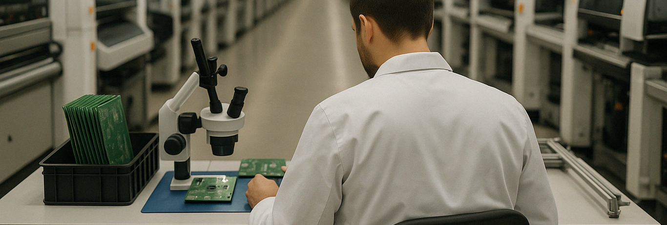
Once soldered, the assembly undergoes a rigorous inspection phase. Automated optical inspection systems scan for defects such as insufficient solder, incorrect part orientation, or missing components. Any issues detected can be routed to rework stations where adjustments are made under strict quality control protocols.
The final stages involve cleaning (if required), applying protective coatings, and conducting final assembly and testing to confirm that the board functions as intended. This may include functional tests, boundary scans, or in-circuit verification, depending on the application. The outcome is a fully functional electronic unit, ready for integration into larger systems or direct deployment.
A complete assembly project extends far beyond the physical process of placing electronic components onto a board. It encompasses every phase from initial PCB fabrication and assembly to system-level integration. For both small and large-scale builds, a detailed workflow is required to ensure accuracy, traceability, and adherence to engineering and manufacturing requirements.
Each project begins with documentation review, including circuit schematics, Bill of Materials (BOM), pick-and-place files, and assembly process guidelines. These documents are used to program equipment, set up production lines, and assign tasks to skilled personnel such as electronic assemblers. Throughout the build, extensive checks are carried out to confirm that components are placed correctly, thermal cycles are validated, and test procedures are aligned with product specifications.
Critical to success is coordination within the supply chain, especially when managing hundreds or thousands of electronic components sourced globally. Components must not only meet functional requirements but must also arrive on time, be traceable, and be stored according to environmental specifications to avoid degradation or damage.
As the product nears completion, cross-functional teams perform system-level evaluations, ensure mechanical fit, load firmware (if applicable), and prepare the assembly for packaging or integration. In sectors such as medical devices or aerospace, additional validation steps may be mandated, including documentation trails and long-term storage simulation. These practices exemplify the thoroughness required in modern electronics manufacturing and highlight the evolution of the manufacturing process from manual techniques to digitally driven operations.
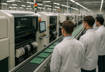
Modern electronic manufacturing facilities rely on an extensive array of equipment to support the assembly process and meet the demand for precision and repeatability. Core tools include soldering equipment, pick-and-place machines, reflow ovens, and inspection systems, each playing a critical role in achieving product quality and functional reliability.
Pick-and-place machines are automated robots that rapidly and accurately place components onto PCBs. These systems operate using vision alignment and precision actuators, achieving placement speeds that range from a few hundred to tens of thousands of parts per hour. For small-batch or prototype runs, semi-automatic equipment or manual placement under magnification may still be employed, especially for custom or irregular components.
Soldering and wiring stations, including automated soldering robots and selective solder machines, provide thermal control and targeting accuracy for surface mount and through-hole components alike. This is essential for meeting the demands of complex electronic assemblies where mixed technologies coexist on densely populated circuit boards.
Equally critical are inspection systems, especially automated optical inspection, which verifies component orientation, solder joint integrity, and alignment. For more advanced validation, X-ray imaging and electrical test stations are deployed to ensure connectivity and performance, particularly in hidden or bottom-terminated packages.
As the industry embraces cutting-edge technology such as AI, machine learning, and Industry 4.0 analytics, many tools now include real-time monitoring, self-calibration, and predictive maintenance capabilities. These innovations contribute to the broader objectives of smart manufacturing and sustainable manufacturing, reducing waste, improving yield, and enhancing traceability across the entire assembly line.
There are several types of electronic assembly processes, each tailored to different design, performance, and manufacturing requirements. These types vary primarily based on the technologies used for placing components onto the PCB, the complexity of the electronic device, and the operational conditions of the final product. Understanding these distinctions is fundamental to choosing the optimal strategy for building electronic assemblies that meet reliability, regulatory, and economic criteria.
The two primary methods are surface mount assembly and through-hole assembly. In surface mount, components are placed directly onto solder-pasted pads on one or both sides of a printed circuit board. This technique supports miniaturization, high-speed automation, and high-density designs, making it ideal for consumer electronics, medical diagnostics, and computing systems.
In contrast, through-hole methods involve inserting component leads through plated holes in the board. The leads are then soldered from the underside, often via wave or selective soldering equipment. While this method consumes more space, it offers superior mechanical bonding and is widely used in applications demanding robustness, such as industrial equipment, power systems, and automotive modules.
A third category mixed-technology assembly blends surface mount and through-hole components on a single board. This approach is often found in complex electronic systems where functionality, form factor, and stress tolerance must coexist. It requires advanced planning and additional process steps but offers unmatched design flexibility.
These types of electronic assembly techniques allow manufacturers to address a broad range of challenges. Selecting the correct method based on the application's voltage, thermal dissipation, vibration exposure, and size constraints ensures not only performance but also long-term product quality and serviceability.
The choice between SMT, through-hole, or hybrid approaches is largely determined by the application domain and desired production volume. SMT (Surface Mount Technology) remains the dominant method in modern electronics manufacturing due to its efficiency, support for automated lines, and compatibility with miniaturized electronic components. It also enables components to be soldered on the opposite side of the board, allowing full two-sided board utilization.
Through-hole assembly, although less space-efficient, offers high mechanical strength and is often preferred for connectors, transformers, and large passive devices. Because of its enhanced resistance to environmental stressors, it is still used in military, aerospace, and heavy industrial applications. This method remains especially relevant in scenarios where electrical connections must endure mechanical strain or thermal cycling.
Hybrid techniques, or mixed-technology assembly, address situations where no single method suffices. These boards may include delicate microcontrollers using surface mount on one side, and large pin headers or relays using through-hole on the other. This requires double-passing through the assembly line or combining automated soldering with manual operations.
Each technique has unique implications for material selection, board layout, and quality control strategy. For example, SMT requires smooth pad finishes and low-profile components, while through-hole tolerates larger components but increases board real estate. Mixed assemblies, meanwhile, demand refined coordination to manage thermal profiles and ensure that early steps do not compromise later ones.
These approaches reflect how electronic contract manufacturers adapt to varying client needs and used in electronic systems with different lifecycles, operational environments, and regulatory constraints. The continual refinement of these methods ensures that designers and production engineers can build boards that balance performance, cost, and manufacturability.
Choosing the appropriate assembly process is critical to achieving both technical and commercial success in electronics manufacturing. Factors influencing this decision include the electronic device's physical size, function, operating environment, expected lifespan, and target market. A misaligned process selection may lead to underperformance, increased rework, or compromised product quality.
For compact, portable devices like smartphones or wearables, surface mount technology is typically the preferred solution due to its support for component miniaturization and high-speed assembly. SMT also allows for enhanced routing efficiency on printed circuit boards, which is especially valuable in high-frequency applications.
In contrast, for high-current or high-power assemblies such as motor controllers or server-grade power supplies, through-hole components are favored. Their ability to carry higher loads and resist mechanical pull-out forces makes them indispensable in such contexts. Devices subject to repetitive movement, vibration, or temperature fluctuation benefit most from this method.
Prototype development may utilize a mix of hand-soldered SMT components, breadboard interfaces, and socketed electronic components, giving engineers the flexibility to experiment with layouts and component combinations. These builds allow for quick iteration and functional validation before committing to full-scale manufacturing.
Additionally, the choice of process may be influenced by logistics, including component availability, cost, lead times, and compatibility with existing production capabilities. Modern electronic manufacturing services providers analyze these variables holistically, aligning each project with a strategy that supports scalability, supply chain stability, and compliance with international quality standards.
Ultimately, the ability to align an assembly method with the functional and physical demands of the electronic product results in reduced failure rates, improved time-to-market, and optimized production efficiency.
The careful handling and precise placement of electronic components represent one of the most critical aspects of the phase of electronic assembly. Whether in prototype development or full-scale pcb assemblies, ensuring mechanical stability, electrical continuity, and proper orientation is essential to achieving long-term performance. The increasing miniaturization of electronic devices only magnifies this challenge, as parts grow smaller while functionality becomes more sophisticated.
During the assembly process, components directly onto the surface of the printed circuit board are placed with either automated pick-and-place equipment or under magnification by skilled technicians. High-speed machines are programmed with exact X-Y coordinates derived from CAD data and board assemblies documentation. These machines use vacuum nozzles and alignment systems to place even the smallest passive or active components, sometimes within tolerances of just a few microns.
Manual placement may still be preferred during early assembly project phases or for unique builds requiring customization. Regardless of the method, ensuring that each electronic component is handled in accordance with anti-static and thermal sensitivity guidelines is vital. Mishandling can result in microfractures, improper contact, or latent failures especially with sensitive integrated circuits or high-frequency components.
To mitigate risk, parts are stored and transported in moisture-controlled packaging, and safety protocols are implemented at every workstation. Once placed, components are temporarily held in position by solder paste, awaiting the thermal bonding step that transforms physical placement into electrical function.
Printed circuit board assembly, commonly abbreviated as PCBA, refers to the entire process of mounting and interconnecting electronic components on a printed circuit board to create a fully operational electronic system. This process is distinct from PCB fabrication, which deals only with the bare board structure. PCBA includes everything from placing necessary components to soldering, inspection, and testing.
The goal of PCBA is to transform design blueprints and BOM data into a consistent, testable hardware platform. The choice of substrate, layer count, and surface finish are foundational, but so too are decisions regarding via structures, pad spacing, and thermal zones all of which affect how components to create the final assembly are mounted and perform.
The pcb assemblies must support high-density integration, thermal management, and signal integrity, particularly in advanced applications such as 5G infrastructure, industrial controls, or compact wearable electronics. Therefore, PCBA requires close coordination between mechanical design, electrical engineering, and manufacturing teams.
As part of this phase of electronic assembly, multiple quality gates are introduced. These may include SPI (solder paste inspection), AOI (automated optical inspection), and X-ray scanning, especially when dealing with components mounted underneath, such as BGA packages. These control steps are essential for verifying not only positional accuracy but also internal integrity of joints and traces.
Through this structured and multidisciplinary approach, PCBA enables scalable, reliable, and cost-effective production of modern electronic hardware, bridging the gap between innovative design and mass deployment.
The controlled application of solder paste is a decisive step in any electronic assembly process. This viscous material, a blend of metal alloy particles and flux, is deposited on the PCB using stencils or jet printing systems. Its function is twofold: it temporarily holds components in place and, upon heating, facilitates the formation of conductive electrical connections.
Stencil printing is the most widely used method for paste deposition. The stencil must match the printed circuit board assembly layout exactly, with proper aperture shapes and thickness to ensure optimal paste volume. This consistency is particularly important in high-density designs, where even slight over- or under-deposition can lead to defects like bridging, tombstoning, or voids.
Following placement, reflow soldering is employed to melt the paste and create solid metallurgical bonds between component leads and pads. Profiles are carefully engineered to accommodate the melting point of the alloy, component thermal limits, and board construction. Reflow ovens may use convection, vapor-phase, or infrared heating depending on the complexity of the build.
For through-hole or mixed-technology boards, additional soldering techniques such as wave or selective soldering are utilized. These methods allow for sequential integration of robust mechanical components after SMT operations. Regardless of the approach, soldering remains a cornerstone of electronics assembly, influencing thermal reliability, signal quality, and long-term product quality.
The continued advancement of automated soldering systems now capable of real-time temperature correction, solder volume measurement, and defect prediction demonstrates how process control and precision engineering define success in every assembly process.
An electronic assembly company plays a vital role in transforming an idea or engineering design into a tangible, tested, and deployable electronic product. These companies operate at the intersection of design, process engineering, and scaled manufacturing, offering infrastructure and expertise necessary to realize both prototypes and production-grade assemblies.
During the early stages of development, such a company often provides technical consultation, advising on material selection, PCB layout optimization, assembly techniques, and Design for Manufacturability (DfM). By anticipating manufacturing constraints and sourcing considerations from the outset, the assembly partner helps reduce rework, accelerate iterations, and increase overall efficiency across the phase of electronic assembly.
In full-scale production, these companies execute the entire electronic assembly process, from placing components to the PCB, through soldering, inspection, and final assembly and testing. Their responsibility includes ensuring that each electronic component is mounted correctly and that every connection performs reliably. This attention to detail is what ultimately safeguards product quality, compliance, and long-term system stability.
Moreover, modern board assemblies require seamless integration of both electrical components and software interfaces. As such, the most capable providers manage not just the mechanical and thermal aspects of the design but also the configuration, testing, and initial programming of embedded systems and microcontrollers.
A contract electronic manufacturing services company offers scalable, high-precision solutions that accommodate clients across industries such as automotive, telecommunications, defense, industrial automation, and consumer goods. These firms specialize in delivering custom pcb assemblies, rapid prototype builds, and end-to-end production tailored to a client’s functional, regulatory, and operational specifications.
Their services often span the entire manufacturing process: materials procurement, cable and harness manufacturing, stencil and fixture development, component placement, automated soldering, and post-process testing. For each assembly project, a contract electronic manufacturer leverages advanced production technologies such as automated optical inspection, selective soldering, and high-resolution imaging to ensure precision and yield.
Furthermore, these providers manage complex supply chains, sourcing necessary components from validated suppliers while navigating global market volatility, lead time challenges, and obsolescence risks. Their logistics expertise ensures that all components to create the final assembly arrive on schedule and meet traceability and quality documentation standards.
These companies also support lifecycle services, including design validation, failure analysis, and end-of-life strategies. As product iterations increase and lifespans shorten, the ability to rapidly adjust assembly lines and shift resources becomes an essential differentiator in the global electronics market.
When selecting an electronic manufacturing services company offering comprehensive support, decision-makers must evaluate more than just technical capability. Factors such as compliance, scalability, traceability, and cross-disciplinary integration define the value of a long-term manufacturing partnership.
End-to-end providers offer an integrated workflow that begins with design support and extends through printed circuit board assembly, testing, and post-sale services. This approach reduces time-to-market and minimizes friction between design, prototyping, and full-scale production. It also enhances accountability, since a single partner assumes responsibility for multiple stages of the product’s development.
A key strength of such firms is their adaptability to project scope and complexity. Whether handling small-volume pilot runs or ongoing high-volume assembly, they provide the same level of quality control, precision, and documentation. Their involvement also facilitates quicker root cause analysis when addressing quality deviations or unforeseen performance anomalies.
Additionally, these providers implement industry-standard certifications and practices such as IPC-A-610 for assembly acceptability and ISO-based quality systems to guarantee compliance. In critical applications, they also support product traceability, serialization, and secure handling of sensitive or proprietary hardware.
Ultimately, working with a capable electronic assembly services provider empowers companies to focus on innovation while delegating the complexities of physical realization to a trusted partner equipped with cutting-edge infrastructure and global supply access.
Maintaining consistent product quality throughout the electronic assembly process is essential for ensuring that devices meet both performance expectations and regulatory standards. Given the complexity and sensitivity of today’s electronic components, even a minor deviation in assembly parameters such as incorrect orientation, improper thermal profile, or misaligned solder joints can result in functional failure or safety concerns.
Effective quality control starts at the design phase and continues through every step of the assembly process. It involves verifying that all necessary components are placed accurately, that components directly onto the surface of the board form clean, conductive joints, and that all mechanical tolerances are respected. This is especially important in high-density layouts, where a single solder bridge or void can compromise signal integrity or lead to thermal stress under operation.
Standardized inspection techniques such as automated optical inspection (AOI) and X-ray analysis are used to monitor board assemblies during and after production. These systems detect issues like insufficient solder volume, lifted leads, and short circuits between traces. Additionally, comprehensive documentation practices ensure that each batch can be traced back to material sources and process parameters, facilitating swift intervention if quality deviations arise.
In many cases, the phase of electronic assembly includes stress tests, thermal cycling, and vibration exposure, particularly for products destined for automotive, aerospace, or industrial applications. Here, ensuring that each electronic component can endure its operational environment is not a matter of preference but a regulatory obligation. Reliability testing combined with electrical connections verification helps validate the full integrity of the pcb assemblies.
The development of a prototype is a critical milestone in any hardware project. It serves as both a design validation tool and a feasibility benchmark for production. In a contract electronic setting, prototyping often represents the first tangible iteration of a design, where theoretical schematics are transformed into functioning hardware via a full but scaled-down assembly process.
Unlike high-speed, high-volume production runs, prototype builds emphasize flexibility and customization. Each build may be subject to revision based on layout, component selection, and real-world testing. The assembler must therefore manage unique challenges, including short BOMs, manual placement and soldering, and integration of non-standard or low-availability parts.
Despite their limited volume, prototypes must still comply with the same technical rigor as finished products. This includes proper electronic component handling, precise soldering techniques, thermal management, and conformance to performance specs. In some cases, prototyping also involves simulation-based testing and pre-certification analysis.
Small-batch builds offer the additional benefit of identifying latent design or process issues before scaling. This helps address any issues early, reducing risk in future production. For companies relying on a contract electronic manufacturing services company, the ability to shift seamlessly from prototype to production is a key differentiator, ensuring continuity and minimizing process redevelopment during scale-up.
Testing is the final safeguard in the manufacturing process, ensuring that all components to create the final system interact as intended. Two widely used techniques in the electronic assembly field are functional testing and in-circuit testing (ICT) each serving distinct but complementary purposes.
In-circuit testing targets the verification of individual electronic components on a printed circuit board assembly, confirming that resistors, capacitors, and semiconductors are placed, oriented, and electrically connected according to design. ICT typically uses a bed-of-nails fixture or flying probe system to apply electrical signals directly to the test points and evaluate resistance, capacitance, isolation, and connectivity.
Functional testing, on the other hand, evaluates the behavior of the entire electronic system under simulated operational conditions. It tests logic flows, communication protocols, power distribution, and reaction to environmental factors. This step is vital in confirming that the system responds correctly under real-world input, including firmware or embedded control software.
Both testing methods are essential for achieving compliance with quality standards and minimizing field failures. When integrated into the assembly line, these tests provide immediate feedback, allowing for rapid isolation of process faults and continuous yield improvement. In mission-critical applications, comprehensive validation—including thermal shock, humidity, and electromagnetic compatibility (EMC) tests—may be required before the product can be approved for market release.
The evolution of electronics manufacturing is increasingly driven by three converging forces: automation, miniaturization, and the continual refinement of assembly technologies. These trends not only respond to consumer demands for more compact, efficient electronic devices, but also improve throughput, traceability, and process stability in modern manufacturing facilities.
Automation has become a defining feature of high-performance assembly lines. From component warehousing and feeding systems to robotic placement and soldering arms and closed-loop inspection systems, smart automation ensures that electronic components are handled with precision, speed, and consistency. This is especially crucial when components directly onto the surface of a printed circuit board must be mounted within tight tolerances to guarantee signal integrity and thermal efficiency.
The trend toward miniaturization has reshaped assembly techniques, especially with the rising prevalence of fine-pitch integrated circuits, high-density interconnects, and 3D board assemblies. These advances demand not only more accurate soldering equipment, but also higher-resolution imaging, adaptive alignment systems, and refined reflow profiling. In response, many electronic assembly manufacturing environments now integrate AI-powered machine vision and real-time analytics to anticipate placement errors or predict material inconsistencies before they result in failure.
Advances in cutting-edge technology also include the adoption of machine learning algorithms that optimize production flow, enhance predictive maintenance scheduling, and automate inspection tolerance setting. These innovations are especially important in high-mix, low-volume environments, where flexibility is as valuable as speed.
As global focus intensifies on environmental responsibility, sustainable manufacturing practices are becoming integral to the electronics assembly sector. Manufacturers are now compelled not only to produce high-quality hardware but also to reduce waste, energy consumption, and environmental footprint across the entire manufacturing process.
One key strategy is material efficiency using optimized pcb assemblies, reducing solder waste, and selecting recyclable or halogen-free substrates. Another is energy-conscious production, where soldering techniques such as reflow soldering in convection ovens are calibrated to minimize thermal loading without compromising electrical connections.
In addition, the longevity and reparability of electronic devices are now considered vital indicators of sustainability. Designing for durability, facilitating rework and upgrades, and minimizing single-use assemblies all contribute to the circular economy model. Some electronic manufacturing services have also begun adopting carbon tracking tools and eco-impact scoring as part of their traceability frameworks.
Efficient assembly further supports sustainability by reducing defects and rework. When components are placed correctly the first time, using optimized paste volumes and precision alignment, the consumption of materials and energy per functional unit decreases. This not only lowers operational costs but also enhances the manufacturer’s environmental compliance posture.
To remain competitive in a rapidly changing technological environment, companies must invest in future-proofing their electronic assembly capabilities. This involves not only embracing current innovations but also anticipating disruptive trends that will reshape the next decade of electronics manufacturing.
Key among these is the growing role of smart manufacturing ecosystems. By linking production data with enterprise resource planning (ERP), quality management systems, and supplier databases, manufacturers can achieve real-time visibility, dynamic scheduling, and proactive decision-making. These intelligent infrastructures allow for faster response to demand fluctuations, quality deviations, or supply chain disruptions.
Another future-facing development is the integration of original equipment capabilities into contract electronic environments. As customers seek one-stop solutions that encompass everything from design assistance to lifecycle support, assembly providers must align their workflows, certifications, and infrastructure accordingly.
Emerging component technologies such as flexible PCBs, embedded passive structures, and system-in-package modules will also demand adaptive tooling and process flexibility. This may include modular soldering equipment, multi-axis placement heads, or hybrid additive/subtractive manufacturing techniques that bridge traditional and emerging paradigms.
Finally, training and upskilling of technical staff remain critical. Even the most advanced automated systems rely on experienced operators and engineers to interpret data, execute precision adjustments, and ensure that evolving electronic assemblies meet both performance and compliance benchmarks.
By integrating innovation, resilience, and adaptability, future-ready manufacturers will be well-positioned to deliver reliable, efficient, and environmentally responsible electronic products even as the demands of the market grow increasingly complex.
The development and execution of a high-quality electronic assembly process represent far more than a series of technical steps. It is a holistic system that combines engineering expertise, process control, material science, and strategic planning. From placing components directly onto the surface of a printed circuit board, to rigorous quality control, testing, and the adoption of cutting-edge technology, each element of the assembly framework plays a vital role in delivering functional, reliable, and scalable electronic products.
In this context, the role of the electronic assembler is evolving. No longer limited to manual tasks, assemblers today must interpret digital instructions, collaborate with automation systems, and uphold critical safety protocols in ever more complex manufacturing environments. Their work ensures that each electronic component is correctly placed and connected to form a cohesive system that performs as designed under real-world conditions.
As global industries continue to innovate, the demand for reliable, flexible, and intelligent electronics assembly solutions grows stronger. This includes not only the ability to produce prototypes and perform high-volume assembly, but also to integrate disciplines such as mechanical design, firmware deployment, and sustainability analysis within the broader manufacturing process.
Looking forward, organizations will need to align with electronic manufacturing services providers who not only deliver technical excellence but who also demonstrate resilience, environmental awareness, and adaptability in the face of global supply challenges and fast-evolving technologies. The integration of smart manufacturing, traceable supply chain systems, and modular production lines will define the next generation of board assemblies.
Ultimately, whether the task is producing consumer devices, medical systems, or advanced industrial equipment, success depends on a comprehensive understanding of assembly techniques, a commitment to product quality, and the seamless orchestration of all components to create reliable, future-ready solutions. The world of electronic assembly stands at a pivotal point where precision, sustainability, and innovation intersect.